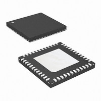
ISL6312CRZ-T Intersil, ISL6312CRZ-T Datasheet - Page 19

ISL6312CRZ-T
Manufacturer Part Number
ISL6312CRZ-T
Description
IC CTRLR PWM 4PHASE BUCK 48-QFN
Manufacturer
Intersil
Datasheet
1.ISL6312CRZ.pdf
(35 pages)
Specifications of ISL6312CRZ-T
Applications
Controller, Intel VR10, VR11, AMD CPU
Voltage - Input
5 ~ 12 V
Number Of Outputs
1
Voltage - Output
0.38 ~ 1.6 V
Operating Temperature
0°C ~ 70°C
Mounting Type
Surface Mount
Package / Case
48-VQFN
Lead Free Status / RoHS Status
Lead free / RoHS Compliant
Available stocks
Company
Part Number
Manufacturer
Quantity
Price
Part Number:
ISL6312CRZ-T
Manufacturer:
INTERSIL
Quantity:
20 000
Company:
Part Number:
ISL6312CRZ-TR5429
Manufacturer:
INTERSIL
Quantity:
101
The ISL6312 incorporates an internal differential
remote-sense amplifier in the feedback path. The amplifier
removes the voltage error encountered when measuring the
output voltage relative to the controller ground reference
point resulting in a more accurate means of sensing output
voltage. Connect the microprocessor sense pins to the
non-inverting input, VSEN, and inverting input, RGND, of the
remote-sense amplifier. The remote-sense output, V
connected to the inverting input of the error amplifier through
an external resistor.
Load-Line (Droop) Regulation
Some microprocessor manufacturers require a
precisely-controlled output resistance. This dependence of
output voltage on load current is often termed “droop” or
“load line” regulation. By adding a well controlled output
impedance, the output voltage can effectively be level shifted
in a direction which works to achieve the load-line regulation
required by these manufacturers.
In other cases, the designer may determine that a more
cost-effective solution can be achieved by adding droop.
Droop can help to reduce the output-voltage spike that
results from fast load-current demand changes.
The magnitude of the spike is dictated by the ESR and ESL
of the output capacitors selected. By positioning the no-load
voltage level near the upper specification limit, a larger
V
OUT
FIGURE 6. OUTPUT VOLTAGE AND LOAD-LINE
R
C
R
FB
C
=
C
V
EXTERNAL CIRCUIT
V
V
REF
OUT
OUT
+
(V
-
DROOP
REGULATION WITH OFFSET ADJUSTMENT
-
+
–
V
OFS
+ V
IDROOP
C
REF
OFS
–
COMP
RGND
VDIFF
VSEN
V
REF
FB
DROOP
)
19
AMPLIFIER
ISL6312 INTERNAL CIRCUIT
ERROR
I
AVG
1k
I
VID DAC
OFS
DIFFERENTIAL
REMOTE-SENSE
AMPLIFIER
+
-
+
-
V
COMP
DIFF
(EQ. 8)
, is
ISL6312
negative spike can be sustained without crossing the lower
limit. By adding a well controlled output impedance, the
output voltage under load can effectively be level shifted
down so that a larger positive spike can be sustained without
crossing the upper specification limit.
As shown in Figure 6, a current proportional to the average
current of all active channels, I
load-line regulation resistor R
across R
creating an output voltage droop with a steady-state value
defined as:
The regulated output voltage is reduced by the droop voltage
V
derived by combining Equations 7, 8, and 9.
In Equation 10, V
programmed offset voltage, I
of the converter, R
connected to the ISEN+ pin, R
is the active channel number, and DCR is the Inductor DCR
value.
Therefore the equivalent loadline impedance, i.e. droop
impedance, is equal to Equation 11:
Output-Voltage Offset Programming
The ISL6312 allows the designer to accurately adjust the
offset voltage by connecting a resistor, R
pin to VCC or GND. When R
and VCC, the voltage across it is regulated to 1.6V. This
causes a proportional current (I
If R
regulated to 0.4V, and I
offset current flowing through the resistor between VDIFF
and FB will generate the desired offset voltage which is
equal to the product (I
shown in Figures 7 and 8.
Once the desired output offset voltage has been determined,
use the following formulas to set R
For Negative Offset (connect R
For Positive Offset (connect R
V
V
R
R
R
DROOP
DROOP
OUT
OFS
OFS
LL
OFS
=
=
=
=
------------
R
is connected to ground, the voltage across it is
. The output voltage as a function of load current is
N
FB
V
--------------------------
V
--------------------------
V
FB
0.4 R
1.6 R
=
OFFSET
OFFSET
REF
I
is proportional to the output current, effectively
⋅
AVG
⋅
⋅
----------------- -
R
DCR
–
FB
FB
ISEN
V
⋅
REF
OFS
ISEN
R
FB
–
is the reference voltage, V
OFS
OFS
⎛
⎜
⎝
is the internal sense resistor
I
------------ -
OUT
N
x R
OFS
flows out of the FB pin. The
OUT
FB
⋅
OFS
FB
AVG
FB
OFS
OFS
----------------- - R
R
. The resulting voltage drop
DCR
). These functions are
ISEN
is connected between OFS
is the total output current
is the feedback resistor, N
, flows from FB through a
OFS
to VCC):
) to flow into the FB pin.
to GND):
⋅
:
OFS
FB
⎞
⎟
⎠
, from the OFS
OFS
February 1, 2011
(EQ. 10)
(EQ. 11)
(EQ. 12)
(EQ. 13)
is the
(EQ. 9)
FN9289.6


