ISL6312CRZ-T Intersil, ISL6312CRZ-T Datasheet - Page 30

ISL6312CRZ-T
Manufacturer Part Number
ISL6312CRZ-T
Description
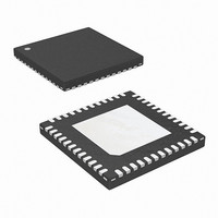
IC CTRLR PWM 4PHASE BUCK 48-QFN
Manufacturer
Intersil
Datasheet
1.ISL6312CRZ.pdf
(35 pages)
Specifications of ISL6312CRZ-T
Applications
Controller, Intel VR10, VR11, AMD CPU
Voltage - Input
5 ~ 12 V
Number Of Outputs
1
Voltage - Output
0.38 ~ 1.6 V
Operating Temperature
0°C ~ 70°C
Mounting Type
Surface Mount
Package / Case
48-VQFN
Lead Free Status / RoHS Status
Lead free / RoHS Compliant
Available stocks
Company
Part Number
Manufacturer
Quantity
Price
Part Number:
ISL6312CRZ-T
Manufacturer:
INTERSIL
Quantity:
20 000
Company:
Part Number:
ISL6312CRZ-TR5429
Manufacturer:
INTERSIL
Quantity:
101
.
Case 3:
The optional capacitor C
noise away from the PWM comparator (see Figure 20). Keep
a position available for C
high-frequency capacitor of between 22pF and 150pF in
case any leading edge jitter problem is noted.
COMPENSATION WITHOUT LOAD-LINE REGULATION
The non load-line regulated converter is accurately modeled
as a voltage-mode regulator with two poles at the L-C
resonant frequency and a zero at the ESR frequency. A
type III controller, as shown in Figure 20, provides the
necessary compensation.
The first step is to choose the desired bandwidth, f
compensated system. Choose a frequency high enough to
assure adequate transient performance but not higher than
1/3 of the switching frequency. The type-III compensator has
an extra high-frequency pole, f
added noise rejection or to assure adequate attenuation at
the error-amplifier high-order pole and zero frequencies. A
good general rule is to choose f
higher if desired. Choosing f
cause problems with too much phase shift below the system
bandwidth.
Case 2:
Case 1:
R
C
------------------------------- -
2 π
C
C
⋅
R
C
------------------------------- -
2 π
f
R
C
⋅
C
C
=
=
0
⋅
1
C
C
>
=
=
R
-------------------------------------------------------------------------------------
(
⋅
L C
2 π
1
=
=
------------------------------------ -
2 π C ESR
FB
R
--------------------------------------------------- -
2 π V
⋅
⋅
L C
⋅
R
----------------------------------------------------------------
2 π V
FB
⋅
⋅
⋅
)
0.66 V
FB
⋅
≤
V
---------------------------------------------------------------- -
2
⋅
2
2
⋅
⋅
0.66 V
f
PP
⋅
, is sometimes needed to bypass
1
, and be prepared to install a
>
0
2 π f
------------------------------------------------------- -
⋅
⋅
f
⋅
PP
<
0
f
⋅
-------------------------------------------- -
0.66 V
⋅
HF
2 π f
2
0
⋅
0.66 V
30
PP
------------------------------------ -
2 π C ESR
(
⋅
⋅
⋅
2 π
0.66 V
IN
⋅
⋅
HF
⋅
V
0.66 V
to be lower than 10f
R
HF
⋅
⋅
0
IN
PP
⋅
⋅
⋅
R
. This pole can be used for
FB
⋅
⋅
⋅
ESR
)
0
FB
V
⋅
= 10f
2
1
IN
IN
⋅
⋅
⋅
⋅
pp
⋅
R
⋅
V
f
⋅
0
IN
⋅
f
FB
IN
pp
f
0
⋅
ESR
⋅
0
2
0
⋅
⋅
⋅
⋅
, but it can be
L C
C
L C
L
⋅
L
L C
⋅
⋅
0
0
, of the
(EQ. 41)
can
ISL6312
In the solutions to the compensation equations, there is a
single degree of freedom. For the solutions presented in
Equation 42, R
compensation components are then selected according to
Equation 42.
In Equation 42, L is the per-channel filter inductance divided
by the number of active channels; C is the sum total of all
output capacitors; ESR is the equivalent-series resistance of
the bulk output-filter capacitance; and V
peak sawtooth signal amplitude as described in “Electrical
Specifications” on page 6.
Output Filter Design
The output inductors and the output capacitor bank together
to form a low-pass filter responsible for smoothing the
pulsating voltage at the phase nodes. The output filter also
must provide the transient energy until the regulator can
respond. Because it has a low bandwidth compared to the
switching frequency, the output filter limits the system
transient response. The output capacitors must supply or
sink load current while the current in the output inductors
increases or decreases to meet the demand.
R
C
C
R
C
FIGURE 21. COMPENSATION CIRCUIT WITHOUT LOAD-LINE
1
1
2
C
C
=
=
=
=
=
C
R
R
------------------------------------------- -
------------------------------------------------------------------------------------------------------------ -
(
---------------------------------------------------------------------------------------- -
0.75 V
------------------------------------------------------------------------------------------------------------ -
(
V
2 π
1
2 π ⋅
1
L C
FB
PP
⋅
⋅
0.75 V
⋅
)
⋅
⋅
)
R
2
------------------------------------------- -
2
–
⎛
⎝
FB
⋅
2π
L C
⋅
IN
REGULATION
C ESR
f
⋅
f
0
⋅
0
FB
⎞
⎠
C ESR
⋅
⋅
⋅
2
⋅
(
IN
f
⋅
f
–
HF
⋅
2 π f
HF
is selected arbitrarily. The remaining
R
f
C ESR
⋅
0
⋅
FB
0.75 V
(
R
⋅
⋅
2 π f
⋅
⋅
C
(
f
⋅
(
HF
⋅
HF
C
L C
L C
⋅
2
⋅
⋅
⋅
⋅
C
L C R
⋅
IN
HF
C
) R
⋅
) R
L C
⋅
⋅
⋅
⋅
⋅
FB
L C
FB
IDROOP
–
FB
COMP
⋅
VDIFF
1
⋅
⋅
)
V
V
–
FB
(
1
(
P P
P P
)
–
PP
–
)
)
is the peak-to-
ISL6312
February 1, 2011
(EQ. 42)
FN9289.6


