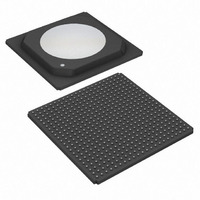
DS34T108GN+ Maxim Integrated Products, DS34T108GN+ Datasheet - Page 14

DS34T108GN+
Manufacturer Part Number
DS34T108GN+
Description
IC TDM OVER PACKET 484HSBGA
Manufacturer
Maxim Integrated Products
Type
TDM (Time Division Multiplexing)r
Datasheet
1.DS34T108GN.pdf
(16 pages)
Specifications of DS34T108GN+
Applications
Data Transport
Mounting Type
Surface Mount
Package / Case
484-BGA Exposed Pad, 484-eBGA, 484-HBGA
Lead Free Status / RoHS Status
Lead free / RoHS Compliant
____________________________________________________ DS34T101, DS34T102, DS34T104, DS34T108
PIN NAME
MII_RX_DV
MII_RX_ERR
MII_COL
MII_CRS
MDC
MDIO
Global Clocks
CLK_SYS_S
CLK_SYS
CLK_CMN
CLK_HIGH
MCLK
CPU Interface
H_CPU_SPI_N
DAT_32_16_N
H_D[31:1]
H_D[0] / SPI_MISO
H_AD[24:1]
H_CS_N
H_R_W_N / SPI_CP
H_WR_BE0_N / SPI_CLK
H_WR_BE1_N / SPI_MOSI
H_WR_BE2_N / SPI_SEL_N
H_WR_BE3_N / SPI_CI
H_READY_N
H_INT[1:0]
JTAG Interface
JTRST_N
JTCLK
JTMS
JTDI
JTDO
Reset and Factory Test Pins
RST_SYS_N
HIZ_N
SCEN
STMD
MBIST_EN
MBIST_DONE
MBIST_FAIL
TEST_CLK
TST_CLD
TST_Tm, TST_Rm
Power and Ground
DVDDC
DVDDIO
DVSS
DVDDLIU
DVSSLIU
ATVDDn
ATVSSn
ARVDDn
ARVSSn
ACVDD1, ACVDD2
ACVSS1, ACVSS2
(1)
TYPE
IOpu
Ipu
Ipu
Ipu
Ipd
Ipu
Ipu
Ipu
Ipd
Ipd
Oz
Oz
IO
IO
O
O
O
O
O
O
P
P
P
P
P
P
P
P
P
P
P
I
I
I
I
I
I
I
I
I
I
I
I
I
I
I
I
I
I
I
(2)
PIN DESCRIPTION
MII Receive Data Valid Input
MII Receive Error Input
MII Collision Input
MII Carrier Sense Input
PHY Management Clock Output
PHY Management Data Input/Output
System Clock Selection Input
System Clock Input: 25, 50 or 75MHz
Common Clock Input (for common clock mode also known as differential mode)
Clock High Input (for adaptive clock recovery machines and E1/T1 master clocks)
Master Clock Input (for E1/T1 master clocks)
Host Bus Interface (1=Parallel Bus, 0=SPI Bus)
Host Data Bus
Host Data LSb or SPI Data Output
Host Address Bus
Host Chip Select (Active Low)
Host Read/Write Control or SPI Clock Phase
Host Write Enable Byte 0 (Active Low) or SPI Clock
Host Write Enable Byte 1 (Active Low) or SPI Data Input
Host Write Enable Byte 2 or SPI Chip Select (Active Low)
Host Write Enable Byte 3 (Active Low) or SPI Clock Invert
Host Ready Output (Active Low)
Host Interrupt Outputs. H_INT[0] for TDMoP. H_INT[1] for LIU and Framer
JTAG Test Reset
JTAG Test Clock
JTAG Test Mode Select
JTAG Test Data Input
JTAG Test Data Output
System Reset (Active Low)
High Impedance Enable (Active Low)
Used for factory tests.
Used for factory tests.
Used for factory tests.
Used for factory tests.
Used for factory tests
Used for factory tests.
Used for factory tests. DS34T104 only.
m = A , B or C. Used for factory tests. DS34T104 only.
1.8V Core Voltage for Framers and TDM-over-Packet Digital Logic (17 pins)
3.3V for I/O Pins (16 pins)
Ground for Framers, TDM-over-Packet and I/O Pins (31 pins)
3.3V for LIU Digital Logic (2 pins)
Ground for LIU Digital Logic (2 pins)
3.3 V for LIU Transmitter Analog Circuits (8pins)
Ground for LIU Transmitter Analog Circuits (8 pins)
3.3 V for LIU Receiver Analog Circuits (8 pins)
Ground for LIU Receiver Analog Circuits (8 pins)
1.8V for CLAD Analog Circuits
Ground for CLAD Analog Circuits
Data Bus Width (1=32-bit , 0=16-bit)
14 of 16


