DS3163 Maxim Integrated Products, DS3163 Datasheet - Page 4
DS3163
Manufacturer Part Number
DS3163
Description
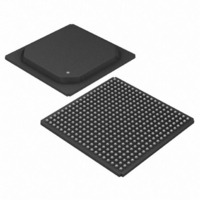
IC TRPL ATM/PACKET PHY 400-PBGA
Manufacturer
Maxim Integrated Products
Datasheet
1.DS3163.pdf
(384 pages)
Specifications of DS3163
Applications
*
Mounting Type
Surface Mount
Package / Case
400-BGA
Lead Free Status / RoHS Status
Lead free / RoHS Compliant
Available stocks
Company
Part Number
Manufacturer
Quantity
Price


9
10
9.1
10.1 P
10.2 C
10.3 R
10.4 G
10.5 P
10.6 UTOPIA/POS-PHY/SPI-3 S
10.7 ATM C
8.3.6
8.3.7
INITIALIZATION AND CONFIGURATION
9.1.1
9.1.2
9.1.3
FUNCTIONAL DESCRIPTION
10.1.1 8/16-Bit Bus Widths.............................................................................................................................. 94
10.1.2 Ready Signal (
10.1.3 Byte Swap Modes ................................................................................................................................ 94
10.1.4 Read-Write/Data Strobe Modes........................................................................................................... 94
10.1.5 Clear on Read/Clear on Write Modes .................................................................................................. 94
10.1.6 Global Write Method ............................................................................................................................ 95
10.1.7 Interrupt and Pin Modes....................................................................................................................... 95
10.1.8 Interrupt Structure ................................................................................................................................ 95
10.2.1 Line Clock Modes................................................................................................................................. 97
10.2.2 Sources of Clock Output Pin Signals ................................................................................................... 98
10.2.3 Line I/O Pin Timing Source Selection .................................................................................................. 99
10.2.4 Clock Structures On Signal IO Pins ................................................................................................... 102
10.2.5 Gapped Clocks................................................................................................................................... 102
10.4.1 Clock Rate Adapter (CLAD)............................................................................................................... 105
10.4.2 8 kHz Reference Generation ............................................................................................................. 107
10.4.3 One-Second Reference Generation .................................................................................................. 109
10.4.4 General-Purpose I/O Pins .................................................................................................................. 109
10.4.5 Performance Monitor Counter Update Details ................................................................................... 111
10.4.6 Transmit Manual Error Insertion ........................................................................................................ 111
10.5.1 Loopbacks.......................................................................................................................................... 112
10.5.2 Loss Of Signal Propagation ............................................................................................................... 114
10.5.3 AIS Logic............................................................................................................................................ 114
10.5.4 Loop Timing Mode ............................................................................................................................. 116
10.5.5 HDLC Overhead Controller ................................................................................................................ 116
10.5.6 Trail Trace .......................................................................................................................................... 117
10.5.7 BERT.................................................................................................................................................. 117
10.5.8 Fractional Payload Controller............................................................................................................. 117
10.5.9 PLCP/Fractional port pins .................................................................................................................. 117
10.5.10 Framing Modes .................................................................................................................................. 121
10.5.11 Mapping Modes.................................................................................................................................. 123
10.5.12 Line Interface Modes.......................................................................................................................... 127
10.6.1 General Description ........................................................................................................................... 128
10.6.2 Features ............................................................................................................................................. 128
10.6.6 System Interface Bus Controller ........................................................................................................ 129
10.7.1 General Description ........................................................................................................................... 134
10.7.2 Features ............................................................................................................................................. 134
10.7.3 Transmit Cell/Packet Processor......................................................................................................... 135
10.7.4 Receive Cell/Packet Processor.......................................................................................................... 135
10.7.5 Cell Processor.................................................................................................................................... 136
10.7.6 Packet Processor ............................................................................................................................... 141
10.7.7 FIFO ................................................................................................................................................... 143
M
ROCESSOR
ER
LOCKS
ESET AND
LOBAL
ONITORING AND
Microprocessor Interface Functional Timing ........................................................................................ 85
JTAG Functional Timing....................................................................................................................... 90
Cell/Packet FIFO.................................................................................................................................. 93
Cell Processor...................................................................................................................................... 93
Packet Processor ................................................................................................................................. 93
P
ORT
ELL
........................................................................................................................................................ 97
R
ESOURCES
R
/ HDLC P
P
ESOURCES
B
OWER
US
D
I
NTERFACE
-D
EBUGGING
RDY
................................................................................................................................... 105
ACKET
OWN
............................................................................................................................... 112
) ............................................................................................................................. 94
.......................................................................................................................... 103
P
......................................................................................................................... 94
YSTEM
ROCESSING
....................................................................................................................... 93
I
NTERFACE
.................................................................................................... 134
........................................................................................... 128
91
94
Related parts for DS3163
Image
Part Number
Description
Manufacturer
Datasheet
Request
R

Part Number:
Description:
MAX7528KCWPMaxim Integrated Products [CMOS Dual 8-Bit Buffered Multiplying DACs]
Manufacturer:
Maxim Integrated Products
Datasheet:
Part Number:
Description:
Single +5V, fully integrated, 1.25Gbps laser diode driver.
Manufacturer:
Maxim Integrated Products
Datasheet:
Part Number:
Description:
Single +5V, fully integrated, 155Mbps laser diode driver.
Manufacturer:
Maxim Integrated Products
Datasheet:
Part Number:
Description:
VRD11/VRD10, K8 Rev F 2/3/4-Phase PWM Controllers with Integrated Dual MOSFET Drivers
Manufacturer:
Maxim Integrated Products
Datasheet:
Part Number:
Description:
Highly Integrated Level 2 SMBus Battery Chargers
Manufacturer:
Maxim Integrated Products
Datasheet:
Part Number:
Description:
Current Monitor and Accumulator with Integrated Sense Resistor; ; Temperature Range: -40°C to +85°C
Manufacturer:
Maxim Integrated Products
Part Number:
Description:
TSSOP 14/A�/RS-485 Transceivers with Integrated 100O/120O Termination Resis
Manufacturer:
Maxim Integrated Products
Part Number:
Description:
TSSOP 14/A�/RS-485 Transceivers with Integrated 100O/120O Termination Resis
Manufacturer:
Maxim Integrated Products
Part Number:
Description:
QFN 16/A�/AC-DC and DC-DC Peak-Current-Mode Converters with Integrated Step
Manufacturer:
Maxim Integrated Products
Part Number:
Description:
TDFN/A/65V, 1A, 600KHZ, SYNCHRONOUS STEP-DOWN REGULATOR WITH INTEGRATED SWI
Manufacturer:
Maxim Integrated Products
Part Number:
Description:
Integrated Temperature Controller f
Manufacturer:
Maxim Integrated Products
Part Number:
Description:
SOT23-6/I�/45MHz to 650MHz, Integrated IF VCOs with Differential Output
Manufacturer:
Maxim Integrated Products
Part Number:
Description:
SOT23-6/I�/45MHz to 650MHz, Integrated IF VCOs with Differential Output
Manufacturer:
Maxim Integrated Products
Part Number:
Description:
EVALUATION KIT/2.4GHZ TO 2.5GHZ 802.11G/B RF TRANSCEIVER WITH INTEGRATED PA
Manufacturer:
Maxim Integrated Products
Part Number:
Description:
QFN/E/DUAL PCIE/SATA HIGH SPEED SWITCH WITH INTEGRATED BIAS RESISTOR
Manufacturer:
Maxim Integrated Products
Datasheet: