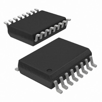
SI8441BB-D-IS Silicon Laboratories Inc, SI8441BB-D-IS Datasheet - Page 15

SI8441BB-D-IS
Manufacturer Part Number
SI8441BB-D-IS
Description
IC ISOLATOR 4CH 5.5V 16-SOIC
Manufacturer
Silicon Laboratories Inc
Series
ISOpror
Datasheet
1.SI8442AB-D-IS.pdf
(38 pages)
Specifications of SI8441BB-D-IS
Number Of Channels
4
Package / Case
16-SOIC (0.300", 7.5mm Width)
Inputs - Side 1/side 2
3/1
Isolation Rating
2500Vrms
Voltage - Supply
2.7 V ~ 5.5 V
Data Rate
150Mbps
Propagation Delay
6ns
Output Type
Tri-State
Operating Temperature
-40°C ~ 125°C
Mounting Style
SMD/SMT
Propagation Delay Time
6 ns
Supply Voltage (max)
5.5 V
Supply Voltage (min)
2.7 V
Supply Current
6 mA
Maximum Operating Temperature
+ 125 C
Minimum Operating Temperature
- 40 C
Lead Free Status / RoHS Status
Lead free / RoHS Compliant
Lead Free Status / RoHS Status
Lead free / RoHS Compliant, Lead free / RoHS Compliant
Other names
336-1762-5
Available stocks
Company
Part Number
Manufacturer
Quantity
Price
Part Number:
SI8441BB-D-IS
Manufacturer:
SILICON LABS/芯科
Quantity:
20 000
Table 6. Regulatory Information*
Table 7. Insulation and Safety-Related Specifications
CSA
The Si84xx is certified under CSA Component Acceptance Notice 5A. For more details, see File 232873.
61010-1: Up to 600 V
60950-1: Up to 130 V
age.
VDE
The Si84xx is certified according to IEC 60747-5-2. For more details, see File 5006301-4880-0001.
60747-5-2: Up to 560 V
UL
The Si84xx is certified under UL1577 component recognition program. For more details, see File E257455.
Rated up to 2500 V
*Note: Regulatory Certifications apply to 2.5 kV
Parameter
Nominal Air Gap (Clearance)
Nominal External Tracking (Creepage)
Minimum Internal Gap (Internal Clearance)
Tracking Resistance
(Proof Tracking Index)
Erosion Depth
Resistance (Input-Output)
Capacitance (Input-Output)
Input Capacitance
Notes:
1. The values in this table correspond to the nominal creepage and clearance values as detailed in “6. Package Outline:
2. To determine resistance and capacitance, the Si84xx is converted into a 2-terminal device. Pins 1–8 are shorted
3. Measured from input pin to ground.
For more information, see "5. Ordering Guide" on page 27.
16-Pin Wide Body SOIC” and “8. Package Outline: 16-Pin Narrow Body SOIC”. VDE certifies the clearance and
creepage limits as 4.7 mm minimum for the NB SOIC-16 package and 8.5 mm minimum for the WB SOIC-16 package.
UL does not impose a clearance and creepage minimum for component level certifications. CSA certifies the clearance
and creepage limits as 3.9 mm minimum for the NB SOIC-16 package and 7.6 mm minimum for the WB SOIC-16
package.
together to form the first terminal and pins 9–16 are shorted together to form the second terminal. The parameters are
then measured between these two terminals.
3
RMS
RMS
RMS
peak
isolation voltage for basic insulation.
2
reinforced insulation working voltage; up to 600 V
reinforced insulation working voltage; up to 1000 V
2
for basic insulation working voltage.
1
1
RMS
rated devices which are production tested to 3.0 kV
Symbol
L(IO1)
L(IO2)
PTI
R
C
ED
Rev. 1.3
C
IO
IO
I
Test Condition
IEC60112
f = 1 MHz
RMS
RMS
Si8440/41/42/45
basic insulation working voltage.
basic insulation working volt-
SOIC-16
0.040
0.008
10
WB
600
8.0
8.0
2.0
4.0
12
Value
RMS
SOIC-16
0.008
0.019
4.01
10
600
NB
4.9
4.0
2.0
for 1 sec.
12
V
Unit
mm
mm
mm
mm
RMS
pF
pF
15


