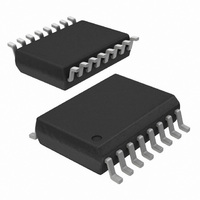
SI8441BB-D-IS Silicon Laboratories Inc, SI8441BB-D-IS Datasheet - Page 20

SI8441BB-D-IS
Manufacturer Part Number
SI8441BB-D-IS
Description
IC ISOLATOR 4CH 5.5V 16-SOIC
Manufacturer
Silicon Laboratories Inc
Series
ISOpror
Datasheet
1.SI8442AB-D-IS.pdf
(38 pages)
Specifications of SI8441BB-D-IS
Number Of Channels
4
Package / Case
16-SOIC (0.300", 7.5mm Width)
Inputs - Side 1/side 2
3/1
Isolation Rating
2500Vrms
Voltage - Supply
2.7 V ~ 5.5 V
Data Rate
150Mbps
Propagation Delay
6ns
Output Type
Tri-State
Operating Temperature
-40°C ~ 125°C
Mounting Style
SMD/SMT
Propagation Delay Time
6 ns
Supply Voltage (max)
5.5 V
Supply Voltage (min)
2.7 V
Supply Current
6 mA
Maximum Operating Temperature
+ 125 C
Minimum Operating Temperature
- 40 C
Lead Free Status / RoHS Status
Lead free / RoHS Compliant
Lead Free Status / RoHS Status
Lead free / RoHS Compliant, Lead free / RoHS Compliant
Other names
336-1762-5
Available stocks
Company
Part Number
Manufacturer
Quantity
Price
Part Number:
SI8441BB-D-IS
Manufacturer:
SILICON LABS/芯科
Quantity:
20 000
Si8440/41/42/45
2.3. Device Operation
Device behavior during start-up, normal operation, and shutdown is shown in Table 12. Table 13 provides an
overview of the output states when the Enable pins are active.
20
Notes:
Input
X
X
X
X
V
1. VDDI and VDDO are the input and output power supplies. V
2. X = not applicable; H = Logic High; L = Logic Low; Hi-Z = High Impedance.
3. It is recommended that the enable inputs be connected to an external logic high or low level when the Si84xx is
4. No Connect (NC) replaces EN1 on Si8440/45. No Connect replaces EN2 on the Si8445. No Connects are not internally
5. “Powered” state (P) is defined as 2.70 V < VDD < 5.5 V.
6. "Unpowered" state (UP) is defined as VDD = 0 V.
7. Note that an I/O can power the die for a given side through an internal diode if its source has adequate current.
8. When using the enable pin (EN) function, the output pin state is driven to a logic low state when the EN pin is disabled
H
L
7
7
7
7
I
1,2
is the enable control input located on the same output side.
operating in noisy environments.
connected and can be left floating, tied to VDD, or tied to GND.
(EN = 0) in Revision C. Revision D outputs go into a high-impedance state when the EN pin is disabled (EN = 0). See
"3. Errata and Design Migration Guidelines" on page 25 for more details.
Input
H or NC
H or NC
H or NC
EN
X
L
L
1,2,3,4
7
State
VDDI
UP
UP
P
P
P
P
1,5,6
Table 12. Si84xx Logic Operation Table
State
VDDO
UP
P
P
P
P
P
1,5,6
Undetermined
V
O
Hi-Z or L
Hi-Z or L
Output
Rev. 1.3
H
L
L
8
8
1,2
I
and V
Enabled, normal operation.
Disabled.
Upon transition of VDDI from unpowered to pow-
ered, V
than 1 µs.
Disabled.
Upon transition of VDDO from unpowered to pow-
ered, V
1 µs, if EN is in either the H or NC state. Upon
transition of VDDO from unpowered to powered,
V
O
O
returns to Hi-Z within 1 µs if EN is L.
are the respective input and output terminals. EN
O
O
returns to the same state as V
returns to the same state as V
Comments
I
I
in less
within


