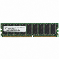
MT9VDDT6472AY-40BF1 Micron Technology Inc, MT9VDDT6472AY-40BF1 Datasheet - Page 24

MT9VDDT6472AY-40BF1
Manufacturer Part Number
MT9VDDT6472AY-40BF1
Description
MODULE DDR SDRAM 512MB 184-DIMM
Manufacturer
Micron Technology Inc
Datasheet
1.MT9VDDT6472AY-40BF1.pdf
(27 pages)
Specifications of MT9VDDT6472AY-40BF1
Memory Type
DDR SDRAM
Memory Size
512MB
Speed
400MT/s
Package / Case
184-DIMM
Lead Free Status / RoHS Status
Lead free / RoHS Compliant
Other names
557-1178
MT9VDDT6472AY-40BF1
MT9VDDT6472AY-40BF1
Table 19: Serial Presence-Detect EEPROM DC Operating Conditions
All voltages referenced to V
Table 20: Serial Presence-Detect EEPROM AC Operating Conditions
All voltages referenced to V
NOTE:
pdf: 09005aef80a43e7d, source: 09005aef80a43d77
DDA9C16_32_64x72AG.fm - Rev. B 9/04 EN
1. To avoid spurious START and STOP conditions, a minimum delay is placed between SCL = 1 and the falling or rising
2. This parameter is sampled.
3. For a reSTART condition, or following a WRITE cycle.
4. The SPD EEPROM WRITE cycle time (
PARAMETER/CONDITION
SUPPLY VOLTAGE
INPUT HIGH VOLTAGE: Logic 1; All inputs
INPUT LOW VOLTAGE: Logic 0; All inputs
OUTPUT LOW VOLTAGE: IOUT = 3mA
INPUT LEAKAGE CURRENT: VIN = GND to VDD
OUTPUT LEAKAGE CURRENT: VOUT = GND to VDD
STANDBY CURRENT: SCL = SDA = VDD - 0.3V; All other inputs = V
POWER SUPPLY CURRENT: SCL clock frequency = 100 KHz
SCL LOW to SDA data-out valid
Time the bus must be free before a new transition can start
Data-out hold time
SDA and SCL fall time
Data-in hold time
Start condition hold time
Clock HIGH period
Noise suppression time constant at SCL, SDA inputs
Clock LOW period
SDA and SCL rise time
SCL clock frequency
Data-in setup time
Start condition setup time
Stop condition setup time
WRITE cycle time
edge of SDA.
the EEPROM internal erase/program cycle. During the WRITE cycle, the EEPROM bus interface circuit is disabled, SDA
remains HIGH due to pull-up resistor, and the EEPROM does not respond to its slave address.
PARAMETER/CONDITION
SS
SS
; V
; V
DDSPD
DDSPD
= +2.3V to +3.6V
= +2.3V to +3.6V
t
WRC) is the time from a valid stop condition of a write sequence to the end of
128MB, 256MB, 512MB (x72, ECC, SR), PC3200
24
DD OR
Micron Technology, Inc., reserves the right to change products or specifications without notice.
V
184-Pin DDR SDRAM UDIMM
SYMBOL
t
t
t
t
t
SS
HD:DAT
HD:STA
SU:DAT
SU:STA
SU:STO
t
t
t
t
HIGH
LOW
f
WRC
t
t
BUF
SCL
AA
DH
t
t
t
F
R
I
SYMBOL
V
V
V
V
I
I
I
I
LO
CC
DD
SB
OL
LI
IH
IL
MIN
200
100
0.2
1.3
0.6
0.6
1.3
0.6
0.6
0
V
DD
MIN
2.3
-1
–
–
–
–
–
x 0.7 V
MAX
300
400
0.9
0.3
50
10
V
DD
DD
UNITS
MAX
KHz
3.6
0.4
10
10
30
ms
2
µs
µs
ns
ns
µs
µs
µs
ns
µs
µs
ns
µs
µs
+ 0.5
x 0.3
©2004 Micron Technology, Inc.
NOTES
UNITS
mA
µA
µA
µA
1
2
2
3
4
V
V
V
V


