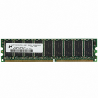
MT9VDDT6472AY-40BF1 Micron Technology Inc, MT9VDDT6472AY-40BF1 Datasheet - Page 8

MT9VDDT6472AY-40BF1
Manufacturer Part Number
MT9VDDT6472AY-40BF1
Description
MODULE DDR SDRAM 512MB 184-DIMM
Manufacturer
Micron Technology Inc
Datasheet
1.MT9VDDT6472AY-40BF1.pdf
(27 pages)
Specifications of MT9VDDT6472AY-40BF1
Memory Type
DDR SDRAM
Memory Size
512MB
Speed
400MT/s
Package / Case
184-DIMM
Lead Free Status / RoHS Status
Lead free / RoHS Compliant
Other names
557-1178
MT9VDDT6472AY-40BF1
MT9VDDT6472AY-40BF1
Burst Length
burst oriented, with the burst length being program-
mable, as shown in Figure 4, Mode Register Definition
Diagram. The burst length determines the maximum
number of column locations that can be accessed for a
given READ or WRITE command. Burst lengths of 2, 4,
or 8 locations are available for both the sequential and
the interleaved burst types.
operation or incompatibility with future versions may
result.
of columns equal to the burst length is effectively
selected. All accesses for that burst take place within
this block, meaning that the burst will wrap within the
block if a boundary is reached. The block is uniquely
selected by A1–Ai when the burst length is set to two,
by A2–Ai when the burst length is set to four and by
A3–Ai when the burst length is set to eight (where Ai is
the most significant column address bit for a given
configuration; see note 5 of Table 6, Burst Definition
Table, on page 9). The remaining (least significant)
address bit(s) is (are) used to select the starting loca-
tion within the block. The programmed burst length
applies to both read and write bursts.
Burst Type
to be either sequential or interleaved; this is referred to
as the burst type and is selected via bit M3.
mined by the burst length, the burst type and the start-
ing column address, as shown in Table 6, Burst
Definition Table, on page 9.
Read Latency
between the registration of a READ command and the
availability of the first bit of output data. The latency
can be set to 3, 2.5, or 2 clocks, as shown in Figure 5,
CAS Latency Diagram, on page 9.
and the latency is m clocks, the data will be available
nominally coincident with clock edge n + m. Table 7,
CAS Latency (CL) Table, on page 9, indicates the oper-
ating frequencies at which each CAS latency setting
can be used.
operation or incompatibility with future versions may
result.
pdf: 09005aef80a43e7d, source: 09005aef80a43d77
DDA9C16_32_64x72AG.fm - Rev. B 9/04 EN
Read and write accesses to DDR SDRAM devices are
Reserved states should not be used, as unknown
When a READ or WRITE command is issued, a block
Accesses within a given burst may be programmed
The ordering of accesses within a burst is deter-
The READ latency is the delay, in clock cycles,
If a READ command is registered at clock edge n,
Reserved states should not be used as unknown
128MB, 256MB, 512MB (x72, ECC, SR), PC3200
8
Operating Mode
MODE REGISTER SET command with bits A7–A11
(128MB), or A7–A12 (256MB, 512MB) each set to zero,
and bits A0–A6 set to the desired values. A DLL reset is
initiated by issuing a MODE REGISTER SET command
with bits A7 and A9–A11 (128MB), or A7 and A9–A12
(256MB, 512MB) each set to zero, bit A8 set to one, and
bits A0–A6 set to the desired values.
* M14 and M13 (BA0 and BA1)
* M13 and M12 (BA0 and BA1)
256MB, 512MB Modules
128MB Module
must be “0, 0” to select the
must be “0, 0” to select the
base mode register (vs. the
base mode register (vs. the
extended mode register).
extended mode register).
The normal operating mode is selected by issuing a
Figure 4: Mode Register Definition
0*
14
BA1
Micron Technology, Inc., reserves the right to change products or specifications without notice.
0*
0*
184-Pin DDR SDRAM UDIMM
13
13
BA1
BA0
0*
12
12
A12 A11
BA0
Operating Mode
11
11
A11
Operating Mode
10
10
A10
A10
M12 M11
0
0
-
9
9
A9
A9
0
0
-
8
8
A8
A8
M10
0
0
-
Diagram
7
7
A7 A6 A5 A4 A3
A7 A6 A5 A4 A3
M9
M6
0
0
-
CAS Latency BT
CAS Latency BT
0
0
0
0
1
1
1
1
6
6
M8 M7
0
1
M5
-
0
0
1
1
0
0
1
1
5
5
0
0
-
M4
0
1
0
1
0
1
0
1
4
4
M3
M6-M0
0
1
Valid
Valid
3
3
-
Burst Length
Burst Length
M2
2
2
0
0
0
0
1
1
1
1
CAS Latency
A2 A1 A0
A2 A1 A0
Reserved
Reserved
Reserved
Reserved
Reserved
M1
0
0
1
1
0
0
1
1
Operating Mode
Normal Operation
Normal Operation/Reset DLL
All other states reserved
1
1
2.5
2
3
M0
0
1
0
1
0
1
0
1
0
0
©2004 Micron Technology, Inc.
Burst Type
Interleaved
Sequential
Reserved
Reserved
Reserved
Reserved
Reserved
Mode Register (Mx)
Mode Register (Mx)
M3 = 0
Address Bus
Address Bus
2
4
8
Burst Length
Reserved
Reserved
Reserved
Reserved
Reserved
M3 = 1
2
4
8


