MT8VDDT6464HDG-335F2 Micron Technology Inc, MT8VDDT6464HDG-335F2 Datasheet - Page 7
MT8VDDT6464HDG-335F2
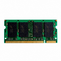
Manufacturer Part Number
MT8VDDT6464HDG-335F2
Description
MODULE DDR 512MB 200-SODIMM
Manufacturer
Micron Technology Inc
Specifications of MT8VDDT6464HDG-335F2
Memory Type
DDR SDRAM
Memory Size
512MB
Speed
333MT/s
Package / Case
200-SODIMM
Main Category
DRAM Module
Sub-category
DDR SDRAM
Module Type
200SODIMM
Device Core Size
64b
Organization
64Mx64
Total Density
512MByte
Chip Density
512Mb
Maximum Clock Rate
333MHz
Operating Supply Voltage (typ)
2.5V
Operating Current
800mA
Number Of Elements
8
Operating Supply Voltage (max)
2.7V
Operating Supply Voltage (min)
2.3V
Operating Temp Range
0C to 70C
Operating Temperature Classification
Commercial
Pin Count
200
Mounting
Socket
Lead Free Status / RoHS Status
Contains lead / RoHS non-compliant


General Description
high-speed CMOS, dynamic random-access, 256MB
and 512MB memory modules organized in x64 config-
uration. DDR SDRAM modules use internally config-
ured quad-bank DDR SDRAMs.
tecture to achieve high-speed operation. The double
data rate architecture is essentially a 2n-prefetch
architecture with an interface designed to transfer two
data words per clock cycle at the I/O pins. A single
read or write access for the DDR SDRAM module effec-
tively consists of a single 2n-bit wide, one-clock-cycle
data transfer at the internal DRAM core and two corre-
sponding n-bit wide, one-half-clock-cycle data trans-
fers at the I/O pins.
externally, along with data, for use in data capture at
the receiver. DQS is an intermittent strobe transmitted
by the DDR SDRAM during READs and by the memory
controller during WRITEs. DQS is edge-aligned with
data for READs and center-aligned with data for
WRITEs.
clock inputs (CK and CK#); the crossing of CK going
HIGH and CK# going LOW will be referred to as the
positive edge of CK. Commands (address and control
signals) are registered at every positive edge of CK.
Input data is registered on both edges of DQS, and out-
put data is referenced to both edges of DQS, as well as
to both edges of CK.
are burst oriented; accesses start at a selected location
and continue for a programmed number of locations
in a programmed sequence. Accesses begin with the
registration of an ACTIVE command, which is then fol-
lowed by a READ or WRITE command. The address
bits registered coincident with the ACTIVE command
are used to select the device bank and row to be
accessed (BA0, BA1 select device bank; A0–A12
(256MB, 512MB) or A0–A13 (1GB) select device row).
The address bits registered coincident with the READ
or WRITE command are used to select the device bank
and the starting device column location for the burst
access.
READ or WRITE burst lengths of 2, 4, or 8 locations. An
auto precharge function may be enabled to provide a
self-timed row precharge that is initiated at the end of
the burst access.
pdf: 09005aef80b575ca, source: 09005aef806e1d28
DDA8C32_64x64HDG.fm - Rev. D 9/04 EN
The MT8VDDT3264HD and MT8VDDT6464HD, are
DDR SDRAM modules use a double data rate archi-
A bidirectional data strobe (DQS) is transmitted
DDR SDRAM modules operate from differential
Read and write accesses to DDR SDRAM modules
DDR SDRAM modules provide for programmable
7
SDRAM modules allows for concurrent operation,
thereby providing high effective bandwidth by hiding
row precharge and activation time.
power-saving power-down mode. All inputs are com-
patible with the JEDEC Standard for SSTL_2. All out-
puts are SSTL_2, Class II compatible.
information regarding DDR SDRAM operation, refer to
the 256Mb or 512Mb DDR SDRAM component data
sheets.
Serial Presence-Detect Operation
detect (SPD). The SPD function is implemented using
a 2,048-bit EEPROM. This nonvolatile storage device
contains 256 bytes. The first 128 bytes can be pro-
grammed by Micron to identify the module type and
various SDRAM organizations and timing parameters.
The remaining 128 bytes of storage are available for
use by the customer. System READ/WRITE operations
between the master (system logic) and the slave
EEPROM device (DIMM) occur via a standard I
using the DIMM’s SCL (clock) and SDA (data) signals,
together with SA (2:0), which provide eight unique
DIMM/EEPROM addresses. Write protect (WP) is tied
to ground on the module, permanently disabling hard-
ware write protect.
Mode Register Definition
mode of operation of DDR SDRAM devices. This defi-
nition includes the selection of a burst length, a burst
type, a CAS latency and an operating mode, as shown
in Figure 4, Mode Register Definition Diagram, on
page 8.
MODE REGISTER SET command (with BA0 = 0 and
BA1 = 0) and will retain the stored information until it
is programmed again or the device loses power (except
for bit A8, which is self-clearing).
contents of the memory, provided it is performed cor-
rectly. The mode register must be loaded (reloaded)
when all device banks are idle and no bursts are in
progress, and the controller must wait the specified
time before initiating the subsequent operation. Vio-
lating either of these requirements will result in
unspecified operation.
A3 specifies the type of burst (sequential or inter-
256MB, 512MB (x64, DR) PC3200
The pipelined, multibank architecture of DDR
An auto refresh mode is provided, along with a
DDR SDRAM modules incorporate serial presence-
The mode register is used to define the specific
Reprogramming the mode register will not alter the
Mode register bits A0–A2 specify the burst length,
Micron Technology, Inc., reserves the right to change products or specifications without notice.
The mode register is programmed via the
200-PIN DDR SODIMM
©2004 Micron Technology, Inc.
For more
2
C bus
Related parts for MT8VDDT6464HDG-335F2
Image
Part Number
Description
Manufacturer
Datasheet
Request
R

Part Number:
Description:
IC SDRAM 64MBIT 133MHZ 54TSOP
Manufacturer:
Micron Technology Inc
Datasheet:

Part Number:
Description:
IC SDRAM 64MBIT 5.5NS 86TSOP
Manufacturer:
Micron Technology Inc
Datasheet:
Part Number:
Description:
IC SDRAM 64MBIT 200MHZ 86TSOP
Manufacturer:
Micron Technology Inc
Datasheet:
Part Number:
Description:
IC SDRAM 64MBIT 133MHZ 54TSOP
Manufacturer:
Micron Technology Inc
Datasheet:
Part Number:
Description:
IC SDRAM 128MBIT 133MHZ 54TSOP
Manufacturer:
Micron Technology Inc
Datasheet:

Part Number:
Description:
IC SDRAM 256MBIT 133MHZ 90VFBGA
Manufacturer:
Micron Technology Inc
Datasheet:
Part Number:
Description:
IC SDRAM 128MBIT 133MHZ 54TSOP
Manufacturer:
Micron Technology Inc
Datasheet:
Part Number:
Description:
IC SDRAM 256MBIT 133MHZ 54TSOP
Manufacturer:
Micron Technology Inc
Datasheet:

Part Number:
Description:
IC DDR SDRAM 512MBIT 6NS 66TSOP
Manufacturer:
Micron Technology Inc
Datasheet:
Part Number:
Description:
IC SDRAM 128MBIT 167MHZ 86TSOP
Manufacturer:
Micron Technology Inc
Datasheet:
Part Number:
Description:
IC SDRAM 128MBIT 143MHZ 86TSOP
Manufacturer:
Micron Technology Inc
Datasheet:

Part Number:
Description:
SDRAM 256M-BIT 1.8V 54-PIN VFBGA
Manufacturer:
Micron Technology Inc
Datasheet:
Part Number:
Description:
IC SDRAM 128MBIT 143MHZ 86TSOP
Manufacturer:
Micron Technology Inc
Datasheet:

Part Number:
Description:
IC SDRAM 128MBIT 125MHZ 54VFBGA
Manufacturer:
Micron Technology Inc
Datasheet:
Part Number:
Description:
IC SDRAM 128MBIT 125MHZ 54VFBGA
Manufacturer:
Micron Technology Inc
Datasheet: