MT9VDDT6472PHG-40BF2 Micron Technology Inc, MT9VDDT6472PHG-40BF2 Datasheet
MT9VDDT6472PHG-40BF2
Specifications of MT9VDDT6472PHG-40BF2


Related parts for MT9VDDT6472PHG-40BF2


MT9VDDT6472PHG-40BF2 Summary of contents
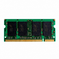
Page 1
... BA1) 4 (BA0, BA1) 256Mb (32 Meg (A0–A9) 1K (A0–A9) 1 (S0#) 1 (S0#) 1 ADVANCE ‡ www.micron.com/products/modules +70°C) A +85° Consult Micron for product availability; indus- trial temperature option available in -265 speed only Device CAS (READ) Latency. 512MB 8K 8K (A0–A12) 16K (A0– ...
Page 2
... MT9VDDT3272PHG-26A_ MT9VDDT3272PHY-26A_ 256MB MT9VDDT3272PH(I)G-265_ 256MB MT9VDDT3272PH(I)Y-265_ 256MB 512MB MT9VDDT6472PHG-335_ MT9VDDT6472PHY-335_ 512MB MT9VDDT6472PHG-262_ 512MB MT9VDDT6472PHY-262_ 512MB 512MB MT9VDDT6472PHG-26A_ MT9VDDT6472PHY-26A_ 512MB MT9VDDT6472PH(I)G-265_ 512MB MT9VDDT6472PH(I)Y-265_ 512MB MT9VDDT12872PHG-335_ MT9VDDT12872PHY-335_ MT9VDDT12872PHG-262_ MT9VDDT12872PHY-262_ MT9VDDT12872PHG-26A_ MT9VDDT12872PHY-26A_ MT9VDDT12872PH(I)G-265_ MT9VDDT12872PH(I)Y-265_ NOTE: All part numbers end with a two-place code (not shown), designating component and PCB revisions. Consult factory for current revision codes ...
Page 3
Table 3: Pin Assignment (200-Pin SODIMM Front) PIN SYMBOL PIN SYMBOL PIN SYMBOL PIN SYMBOL 101 REF DQ19 103 SS 5 DQ0 55 DQ24 105 7 DQ1 57 V 107 DD 9 ...
Page 4
Table 5: Pin Descriptions Refer to Pin Assignment Tables on page 3 for pin number and symbol correlation. PIN NUMBERS SYMBOL 118, 119, 120 WE#, CAS#, RAS# 35, 37 CK0, CK0# 96 CKE0, 121 117, 116 BA0, BA1 99 (A12), ...
Page 5
Table 5: Pin Descriptions Refer to Pin Assignment Tables on page 3 for pin number and symbol correlation. PIN NUMBERS SYMBOL 13, 14, 17, 18, DQ0–DQ63 19, 20, 23, 24, 29, 30, 31, 32, 41, 42, ...
Page 6
... RAS# CAS# CKE0 WE# NOTE: 1. All resistor values are 22 unless otherwise specified. 2. Per industry standard, Micron modules utilize various component speed grades, as referenced in the module part numbering guide at . www micron.com/numberguide. pdf: 09005aef808ffe58, source: 09005aef808ffdc7 DD9C16_32_64_128x72PHG.fm - Rev. B 9/04 EN 128MB, 256MB, 512MB, 1GB (x72, ECC, PLL, SR) ...
Page 7
... DDR SDRAM modules use internally configured quad-bank DDR SDRAM devices. DDR SDRAM modules use a double data rate archi- tecture to achieve high-speed operation. The double data rate architecture is essentially a 2n-prefetch architecture with an interface designed to transfer two data words per clock cycle at the I/O pins ...
Page 8
... Figure 4: Mode Register Definition 128MB Module BA1 M13 and M12 (BA0 and BA1) must be “0, 0” to select the base mode register (vs. the extended mode register). 256MB and 512MB Modules BA1 BA0 M14 and M13 (BA0 and BA1) must be “0, 0” to select the base mode register (vs ...
Page 9
Table 6: Burst Definition Table ORDER OF ACCESSES WITHIN STARTING BURST COLUMN TYPE = LENGTH ADDRESS SEQUENTIAL 0 0-1-2 1-2-3 2-3-0 3-0-1 ...
Page 10
... READ command can be issued. pdf: 09005aef808ffe58, source: 09005aef808ffdc7 DD9C16_32_64_128x72PHG.fm - Rev. B 9/04 EN 128MB, 256MB, 512MB, 1GB (x72, ECC, PLL, SR) 200-PIN DDR SDRAM SODIMM Figure 6: Extended Mode Register 128MB Module BA1 BA0 256MB and 512MB Modules BA1 BA0 1GB Module BA1 BA0 A13 The 15 ...
Page 11
Commands Table 8, Commands Truth Table, and Table 9, DM Operation Truth Table, provide a general reference of available commands. For a more detailed description Table 8: Commands Truth Table CKE is HIGH for all commands shown except SELF REFRESH; ...
Page 12
Absolute Maximum Ratings Stresses greater than those listed may cause perma- nent damage to the device. This is a stress rating only, and functional operation of the device at these or any other conditions above those indicated in the opera- ...
Page 13
Table 12: I Specifications and Conditions – 128MB DD DDR SDRAM components only; Notes: 1–5, 8, 10, 12, 47; notes appear on pages 19–22; 0°C PARAMETER/CONDITION OPERATING CURRENT: One device bank; Active-Precharge (MIN); ...
Page 14
Table 13: I Specifications and Conditions – 256MB DD DDR SDRAM components only; Notes: 1–5, 8, 10, 12, 47; notes appear on pages 19–22; 0°C PARAMETER/CONDITION OPERATING CURRENT: One device bank; Active-Precharge (MIN); ...
Page 15
Table 14: I Specifications and Conditions – 512MB DD DDR SDRAM components only; Notes: 1–5, 8, 10, 12, 47; notes appear on pages 19–22; 0°C PARAMETER/CONDITION OPERATING CURRENT: One device bank; Active-Precharge (MIN ...
Page 16
Table 15: I Specifications and Conditions – 1GB DD DDR SDRAM components only; Notes: 1–5, 8, 10, 12, 47; notes appear on pages 19–22; 0°C PARAMETER/CONDITION OPERATING CURRENT: One device bank; Active-Precharge (MIN ...
Page 17
Table 16: Capacitance) Note: 11; notes appear on pages 19–22 PARAMETER Input/Output Capacitance: DQ, DQS, DM Input Capacitance: Command and Address, S#, CKE Input Capacitance: CK, CK# Table 17: Electrical Characteristics and Recommended AC Operating Conditions DDR SDRAM components only; ...
Page 18
Table 17: Electrical Characteristics and Recommended AC Operating Conditions (Continued) DDR SDRAM components only; notes appear on pages 19–22 AC CHARACTERISTICS PARAMETER DQ-DQS hold, DQS to first non- valid, per access Data Hold Skew Factor ACTIVE to ...
Page 19
Notes 1. All voltages referenced Tests for AC timing and electrical AC and DC DD characteristics may be conducted at nominal ref- erence/supply voltage levels, but the related spec- ifications and device operation are ...
Page 20
However, an AUTO REFRESH command must be asserted at least once every 140.6µs (128MB) or 70.3µs (256MB, 512MB, 1GB); burst refreshing or posting by the DRAM controller greater than eight refresh cycles is not allowed. 22. The ...
Page 21
HP min is the lesser of CL minimum and t minimum actually applied to the device CK and CK# inputs, collectively during bank active. 31. READs and WRITEs with auto precharge are not t allowed to be ...
Page 22
Random addressing changing and 50 percent of data changing at every transfer. 42. Random addressing changing and 100 percent of data changing at every transfer. 43. CKE must be active (high) during the entire time a refresh command is ...
Page 23
Initialization To ensure device operation the DRAM must be ini- tialized as described below: 1. Simultaneously apply power Apply V and then V power. REF TT 3. Assert and hold CKE at a LVCMOS logic low. 4. ...
Page 24
... NOTE: 1. The timing and switching specifications for the PLL listed above are critical for proper operation of DDR SDRAM modules. These are meant subset of the parameters for the specific device used on the module. Detailed information for this PLL is available in JEDEC Standard JESD82. ...
Page 25
... NOTE: 1. Micron Technology, Inc. recommends a minimum air flow of 1 meter/second (~197 LFM) across all modules. 2. The component case temperature measurements shown above were obtained experimentally. The typical system to be used for experimental purposes is a dual-processor 600 MHz work station, fully loaded, with four comparable registered memory modules ...
Page 26
SPD Clock and Data Conventions Data states on the SDA line can change only during SCL LOW. SDA state changes during SCL HIGH are reserved for indicating start and stop conditions (as shown in Figure 12, Data Validity, and Figure ...
Page 27
Table 19: EEPROM Device Select Code Most significant bit (b7) is sent first SELECT CODE Memory Area Select Code (two arrays) Protection Register Select Code Table 20: EEPROM Operating Modes MODE RW BIT Current Address Read 1 Random Address Read ...
Page 28
Table 21: Serial Presence-Detect EEPROM DC Operating Conditions All voltages referenced DDSPD PARAMETER/CONDITION SUPPLY VOLTAGE INPUT HIGH VOLTAGE: Logic 1; All inputs INPUT LOW VOLTAGE: Logic 0; All inputs OUTPUT LOW VOLTAGE 3mA ...
Page 29
Table 23: Serial Presence-Detect Matrix – 128MB, 256MB, 512MB “1”/”0”: Serial Data, “driven to HIGH”/”driven to LOW” BYTE DESCRIPTION 0 Number of SPD Bytes Used by Micron 1 Total Number of Bytes in SPD Device 2 Fundamental Memory Type 3 ...
Page 30
... The value of RP, RCD, and RAP for -335 modules indicated as 18ns to align with industry specifications; actual DDR SDRAM device specification is 15ns. pdf: 09005aef808ffe58, source: 09005aef808ffdc7 DD9C16_32_64_128x72PHG.fm - Rev. B 9/04 EN 128MB, 256MB, 512MB, 1GB (x72, ECC, PLL, SR) 200-PIN DDR SDRAM SODIMM ENTRY(VERSION ...
Page 31
Table 24: Serial Presence- Detect Matrix – 1GB “1”/”0”: Serial Data, “driven to HIGH”/”driven to LOW” BYTE DESCRIPTION 0 Number of SPD Bytes Used by Micron 1 Total Number of Bytes in SPD Device 2 Fundamental Memory Type 3 Number ...
Page 32
... The value of RP, RCD, and RAP for -335 modules indicated as 18ns to align with industry specifications; actual DDR SDRAM device specification is 15ns. pdf: 09005aef808ffe58, source: 09005aef808ffdc7 DD9C16_32_64_128x72PHG.fm - Rev. B 9/04 EN 128MB, 256MB, 512MB, 1GB (x72, ECC, PLL, SR) 200-PIN DDR SDRAM SODIMM ENTRY(VERSION) ...
Page 33
Figure 16: 200-Pin SODIMM Dimensions 0.079 (2.00) R (2X) U1 0.071 (1.80) (2X) 0.236 (6.00) 0.096 (2.44) 0.079 (2.00) 0.039 (0.99) U6 PIN 200 NOTE: All dimensions are in inches (millimeters); Data Sheet Designation Advance: This datasheet contains initial descrip- ...