AFBR-57M5APZ Avago Technologies US Inc., AFBR-57M5APZ Datasheet
AFBR-57M5APZ
Specifications of AFBR-57M5APZ
517-1713
517-1713
Available stocks


Related parts for AFBR-57M5APZ


AFBR-57M5APZ Summary of contents
Page 1
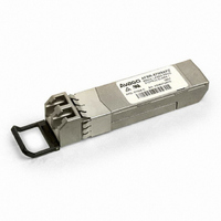
... Ethernet, RoHS Compliant Optical Transceiver Data Sheet 850 nm, SFP (Small Form Pluggable), RoHS Compliant, Low Voltage (3.3 V) Digital Diagnostic Optical Transceiver Description Avago’s AFBR-57M5APZ optical transceiver supports high- speed serial links over multimode optical fiber at signaling rates up to 2.125 Gb/s. Compliant with Small Form Plug- gable (SFP) Multi Source Agreement (MSA) mechanical and electrical specifications for LC Duplex transceivers, ANSI Fibre Channel FC-PI, FC-PI-2 and compliant with IEEE 802 ...
Page 2
... The digital diagnostic interface also adds the ability to disable the transmitter (TX_DISABLE), monitor for Trans- mitter Faults (TX_FAULT), and monitor for Receiver Loss of Signal (RX_LOS). Installation The AFBR-57M5APZ can be installed in any SFF-8074i compliant Small Form Pluggable (SFP) port regardless of host equipment operating status. The AFBR-57M5APZ is hot-pluggable, allowing the module to be installed while the host system is operating and on-line. Upon insertion, the transceiver housing makes initial contact with the host board SFP cage, mitigating potential damage due to Electro-Static Discharge (ESD) ...
Page 3
... The TX_FAULT will be latched high when a laser fault occurs and is cleared by toggling the TX_DISABLE input or power cycling the transceiver. The transmitter fault condition can also be monitored via the two-wire serial interface (address A2, byte 110, bit 2). Eye Safety Circuit The AFBR-57M5APZ provides Class 1 (single fault tolerant) eye safety by design and has been tested for compliance with the requirements listed in Table 1. The eye safety circuit continuously monitors the optical output power level and will disable the transmitter upon detecting an unsafe condition beyond the scope of Class 1 certifica- tion. Such unsafe conditions can be due to inputs from the host board (Vcc fluctuation, unbalanced code fault within the transceiver ...
Page 4
... Rx_LOS thresholds are factory set so that a high output indicates a definite optical fault has occurred. Rx_LOS can also be monitored via the two-wire serial interface (address A2h, byte 110, bit 1). Functional Data I/O The AFBR-57M5APZ interfaces with the host circuit board through twenty I/O pins (SFP electrical connector) identified by function in Table 2. The board layout for this interface is depicted in Figure 6. The AFBR-57M5APZ high speed transmit and receive interfaces require SFP MSA compliant signal lines on the host board ...
Page 5
... Electromagnetic Interference (EMI) Equipment incorporating gigabit transceivers is typically subject to regulation by the FCC in the United States, CENELEC EN55022 (CISPR 22) in Europe and VCCI in Japan. The AFBR-57M5APZ’s compliance to these standards is detailed in Table 1. The metal housing and shielded design of the AFBR-57M5APZ minimizes the EMI challenge facing the equipment designer. EMI Immunity (Susceptibility) Due to its shielded design, the EMI immunity of the AFBR- 57M5APZ exceeds typical industry standards ...
Page 6
Tx_DISABLE Tx_FAULT SERDES IC PROTOCOL IC LOSS OF SIGNAL 4 kΩ MODULE DETECT SCL SDA Figure 2. Typical application configuration 0.1 µ 0.1 µF 10 µF SFP MODULE HOST BOARD NOTE: INDUCTORS MUST HAVE LESS ...
Page 7
Table 2. Pin Description Pin Name Function/Description 1 VeeT Transmitter Ground 2 TX_FAULT Transmitter Fault Indication – High indicates a fault condition 3 TX_DISABLE Transmitter Disable – Module electrical input disables on high or open 4 MOD-DEF2 Module Definition 2 – Two wire serial ID interface data line (SDA) 5 MOD-DEF1 Module Definition 1 – Two wire serial ID interface clock line (SCL) 6 MOD-DEF0 Module Definition 0 – Grounded in module (module present indicator) 7 N.C. 8 RX_LOS Loss of Signal – High indicates loss of received optical signal 9 VeeR Receiver Ground 10 VeeR Receiver Ground 11 VeeR Receiver Ground 12 RD- ...
Page 8
Table 3. Absolute Maximum Ratings Parameter Storage Temperature Case Operating Temperature Relative Humidity Supply Voltage Low Speed Input Voltage Notes; 1. Absolute Maximum Ratings are those values beyond which damage to the device may occur if these limits are exceeded for other than a short period of time. See Reliability Data Sheet for specific reliability performance. 2. Between Absolute Maximum Ratings and the Recommended Operating Conditions functional performance is not intended, device reliability is not implied, and damage to the device may occur over an extended period of time. 3. The module supply voltages and Table 4. Recommended Operating Conditions Parameter Case Operating Temperature Supply Voltage Data Rate Notes: 1. The Ambient Operating Temperature limitations are based on the Case Operating Temperature limitations and are subject to the host system thermal design. 2. Recommended Operating Conditions are those values for which functional performance and device reliability is implied. Table 5. Transceiver Electrical Characteristics (T = -10°C to 85°C, VccT, VccR = 3.3 V ±10%) C Parameter AC Electrical Characteristics Power Supply Noise Rejection (peak-peak) ...
Page 9
Table 6. Transmitter and Receiver Electrical Characteristics (T = -10°C to 85°C, VccT, VccR = 3.3 V ±10%) C Parameter High Speed Data Input: Transmitter Differential Input Voltage (TD +/-) High Speed Data Output: Receiver Differential Output Voltage (RD +/-) Receiver Contributed Total Jitter (2.125 Gb/s) Receiver Contributed Total Jitter (1.0625 Gb/s) Receiver Contributed Total Jitter (1.25 Gb/s) Receiver Electrical Output Rise & Fall Times (20-80%) Notes: 1. Internally AC coupled and terminated (100 Ohm differential). 2. Internally AC coupled but requires an external load termination (100 Ohm differential). 3. Contributed DJ is measured on an oscilloscope in average mode with 50% threshold and K28.5 pattern. Contributed TJ is the sum of contrib- uted RJ and contributed DJ. Contributed RJ is calculated for 1x10 from the oscilloscope by 14. Per FC-PI (Table jitter output, note 1), the actual contributed RJ is allowed to increase above its limit if the actual contributed DJ decreases below its limits, as long as the component output DJ and TJ remain within their specified FC-PI maximum lim- its with the worst case specified component jitter input. 4. 20%-80% electrical rise & fall times measured with a 500 MHz signal utilizing a 1010 data pattern. 9 Symbol ...
Page 10
Table 7. Transmitter Optical Characteristics (T = -10°C to 85°C, VccT, VccR = 3.3V ±10%) C Parameter Modulated Optical Output Power (OMA) (Peak-to-Peak) 2.125 Gb/s Modulated Optical Output Power (OMA) (Peak-to-Peak) 1.0625 Gb/s Average Optical Output Power Optical Extinction Ratio Center Wavelength Spectral Width – rms Optical Rise/Fall Time (2.125 Gb/s) RIN (OMA) 12 Transmitter Contributed Total Jitter (2.125 Gb/s) Transmitter Contributed Total Jitter (1.0625 Gb/s) Transmitter Contributed Total Jitter (1.25 Gb/s) Pout TX_DISABLE Asserted Notes OMA of 196 µW is approximately equal to an average power of –9 dBm, avg assuming an Extinction Ratio OMA of 156 µW is approximately equal to an average power of –10 dBm, avg assuming an Extinction Ratio of 9 dB. 3. Max Pout is the lesser of Class 1 safety limits (CDRH and EN 60825) or receiver power, max. 4. Into 50/125 µm (0.2 NA) multi-mode optical fiber. 5. Contributed DJ is measured on an oscilloscope in average mode with 50% threshold and K28.5 pattern. Contributed TJ is the sum of contrib- uted RJ and contributed DJ. Contributed RJ is calculated for 1x10 from the oscilloscope by 14. Per FC-PI (Table jitter output, note 1), the actual contributed RJ is allowed to increase above its limit if the actual contributed DJ decreases below its limits, as long as the component output DJ and TJ remain within their specified FC-PI maximum limits with the worst case specified component jitter input. 10 ...
Page 11
Table 8. Receiver Optical Characteristics (T = -10°C to 85°C, VccT, VccR = 3.3 V ±10%) C Parameter Input Optical Power [Overdrive] Input Optical Modulation Amplitude (Peak-to-Peak) 2.125 Gb/s [Sensitivity] Input Optical Modulation Amplitude (Peak-to-Peak) 1.0625 Gb/s [Sensitivity] Receiver Sensitivity (Optical Input Power) Stressed Receiver Sensitivity (OMA) 2.125 Gb/s Stressed Receiver Sensitivity (OMA) 1.0625 Gb/s Stressed Receiver Sensitivity (OMA) 1.25 Gb/s Return Loss Bit Error Rate Loss of Signal – Assert Loss of Signal - De-Assert Loss of Signal Hysteresis Notes: 1. Input Optical Modulation Amplitude (commonly known as sensitivity) requires a valid 8B/10B encoded input OMA of 49 µW is approximately equal to an average power of –15 dBm, avg with an Extinction Ratio OMA of 31 µW is approximately equal to an average power of –17 dBm, avg with an Extinction Ratio of 9 dB. 4. 2.125 Gb/s stressed receiver vertical eye closure penalty (ISI) min. is 1.26 dB for 50 µm fiber and 2.03 dB for 62.5 µm fiber. Stressed receiver DCD component min. (at TX ps. 5. ...
Page 12
Table 9. Transceiver SOFT DIAGNOSTIC Timing Characteristics (T = -10°C to 85°C, VccT, VccR = 3.3 V ±10%) C Parameter Hardware TX_DISABLE Assert Time Hardware TX_DISABLE Negate Time Time to initialize, including reset of TX_FAULT Hardware TX_FAULT Assert Time Hardware TX_DISABLE to Reset Hardware RX_LOS DeAssert Time Hardware RX_LOS Assert Time Software TX_DISABLE Assert Time Software TX_DISABLE Negate Time Software Tx_FAULT Assert Time Software Rx_LOS Assert Time Software Rx_LOS De-Assert Time Analog parameter data ready Serial bus hardware ready Write Cycle Time Serial ID Clock Rate Notes: 1. Time from rising edge of TX_DISABLE to when the optical output falls below 10% of nominal. 2. Time from falling edge of TX_DISABLE to when the modulated optical output rises above 90% of nominal. 3. Time from power on or falling edge of Tx_Disable to when the modulated optical output rises above 90% of nominal. 4. From power on or negation of TX_FAULT using TX_DISABLE. 5. Time TX_DISABLE must be held high to reset the laser fault shutdown circuitry. 6. Time from loss of optical signal to Rx_LOS Assertion. 7. Time from valid optical signal to Rx_LOS De-Assertion. 8. Time from two-wire interface assertion of TX_DISABLE (A2h, byte 110, bit 6) to when the optical output falls below 10% of nominal. Measured from falling clock edge after stop bit of write transaction. 9. ...
Page 13
Table 10. Transceiver Digital Diagnostic Monitor (Real Time Sense) Characteristics (T = -10°C to 85°C, VccT, VccR = 3.3 V ±10%) C Parameter Transceiver Internal Temperature Accuracy Transceiver Internal Supply Voltage Accuracy Transmitter Laser DC Bias Current Accuracy Transmitted Average Optical Output Power Accuracy Received Average Optical Input Power Accuracy V T,R > 2. TX_FAULT TX_DISABLE TRANSMITTED SIGNAL t_init t-init: TX DISABLE NEGATED V T,R > 2. TX_FAULT TX_DISABLE TRANSMITTED ...
Page 14
... Link distance with 62.5/125 µm cable at 1.0625 GBit/sec is 300 m. Link distance with 62.5/125 µm cable at 2.125 GBit/sec is 150 m. 4. The IEEE Organizationally Unique Identifier (OUI) assigned to Avago Technologies is 00-17-6A (3 bytes of hex). 5. Laser wavelength is represented in 16 unsigned bits. The hex representation of 850 (nm) is 0352. 6. Addresses 63 and 95 are checksums calculated (per SFF-8472 and SFF-8074) and stored prior to product shipment. 7. Addresses 68-83 specify the AFBR-57M5APZ ASCII serial number and will vary on a per unit basis. 8. Addresses 84-91 specify the AFBR-57M5APZ ASCII date code and will vary on a per date code basis. 14 Byte # Data Decimal Hex ...
Page 15
... Temperature (Temp) is decoded bit signed twos compliment integer in increments of 1/256°C. 2. Supply Voltage (Vcc) is decoded bit unsigned integer in increments of 100 µV. 3. Laser bias current (Tx Bias) is decoded bit unsigned integer in increments of 2 µA. 4. Transmitted average optical power (Tx Pwr) is decoded bit unsigned integer in increments of 0.1 µW. 5. Received average optical power (Rx Pwr) is decoded bit unsigned integer in increments of 0.1 µW. 6. Bytes 56-94 are not intended for use with AFBR-57M5APZ, but have been set to default values per SFF-8472. 7. Byte checksum calculated (per SFF-8472) and stored prior to product shipment. 15 Byte # ...
Page 16
... Indicates transceiver is powered and real time sense data is ready Ready) Notes: 1. The response time for soft commands of the AFBR-57M5APZ is 100 msec as specified by the MSA SFF-8472. 2. Bit 6 is logic OR’d with the SFP TX_DISABLE input pin 3 ... either asserted will disable the SFP transmitter. 3. AFBR-57M5APZ meets the MSA SFF-8472 data ready timing of 1000 msec. 4. Status bits do not impact optical performance. Table 14. EEPROM Serial ID Memory Contents – Alarms and Warnings (Address A2h, Bytes 112, 113, 116, 117) Byte Bit ...
Page 17
Figure 5. Module drawing. 17 ...
Page 18
X Y 16.25 MIN. PITCH B PCB EDGE 5.68 8.58 11.08 16.25 REF. 14.25 2.0 11x 3 3.2 PIN 1 10.93 9.6 0.8 TYP 1.55 ± 0.05 ∅ 0 DETAIL 1 Figure 6. SFP host board mechanical layout. ...
Page 19
MAX. 11.73 REF 9.8 MAX. PCB Figure 7. SFP Assembly drawing. Tcase REFERENCE POINT 15.25 ± 0.1 10 REF (to PCB) 16.25 ± 0.1 MIN. PITCH 0.4 ± 0.1 (below PCB) DIMENSIONS ARE IN ...
Page 20
Customer Manufacturing Processes This module is pluggable and is not designed for aqueous wash, IR reflow, or wave soldering processes. For product information and a complete list of distributors, please go to our website: Avago, Avago Technologies, and the A logo are trademarks of Avago Technologies Limited in the United States and other countries. Data subject to ...