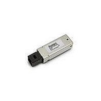
AFBR-5921ALZ Avago Technologies US Inc., AFBR-5921ALZ Datasheet - Page 8

AFBR-5921ALZ
Manufacturer Part Number
AFBR-5921ALZ
Description
TXRX SSF 3.3V 2/1GBS PTH 2X5
Manufacturer
Avago Technologies US Inc.
Series
-r
Datasheet
1.AFBR-5921ALZ.pdf
(13 pages)
Specifications of AFBR-5921ALZ
Data Rate
2.125Gbps
Wavelength
850nm
Applications
General Purpose
Voltage - Supply
2.97 V ~ 3.63 V
Connector Type
LC Duplex
Mounting Type
Through Hole
Function
SFF, PTH, Low Voltage 3.3 V, Optical Transceiver for Fibre Channel
Product
Transceiver
Maximum Rise Time
0.15 ns/0.2 ns
Maximum Fall Time
0.15 ns/0.2 ns
Pulse Width Distortion
0.063 ns (Max)/0.076 ns (Max)
Operating Supply Voltage
2.97 V to 3.63 V
Maximum Operating Temperature
+ 85 C
Minimum Operating Temperature
- 10 C
Package / Case
DIP With Connector
Lead Free Status / RoHS Status
Lead free / RoHS Compliant
For Use With
Multimode Glass
Lead Free Status / RoHS Status
Lead free / RoHS Compliant, Lead free / RoHS Compliant
Available stocks
Company
Part Number
Manufacturer
Quantity
Price
Company:
Part Number:
AFBR-5921ALZ
Manufacturer:
Avago Technologies
Quantity:
135
Table 7. Transmitter and Receiver Electrical Characteristics
(T
Notes:
1. Internally AC coupled and terminated (100 Ohm differential). These levels are compatible with CML and LVPECL voltage swings.
2. Internally AC coupled with internal 50 ohm pullups to V
3. 20%-80% Rise and Fall times measured with a 500 MHz signal utilizing a 1010 data pattern.
4. Contributed DJ is measured on an oscilloscope in average mode with 50% threshold and K28.5 pattern.
5. Contributed RJ is calculated for 1E-12 BER by multiplying the RMS jitter (measured on a single rise or fall edge) from the oscilloscope by 14. Per
6. In a network link, each component’s output jitter equals each component’s input jitter combined with each component’s contributed jitter.
7. Please refer to the AFBR-5921ALZ Characterization Report for typical values.
8
Parameter
Data Input:
Transmitter Differential Input
Voltage (TD +/–)
Data Output:
Receiver Differential Output
Voltage (RD +/–)
Receive Data Rise and Fall
Times (Receiver)
Contributed Deterministic Jitter
(Receiver) 2.125 Gb/s
Contributed Deterministic Jitter
(Receiver) 1.0625 Gb/s
Contributed Random Jitter
(Receiver) 2.125 Gb/s
Contributed Random Jitter
(Receiver) 1.0625 Gb/s
C
the FC-PI standard (Table 13 - MM jitter output, note 1), the actual contributed RJ is allowed to increase above its limit if the actual contributed
DJ decreases below its limits, as long as the component output DJ and TJ remain within their specified FC-PI maximum limits with the worst case
specified component jitter input.
Contributed DJ adds in a linear fashion and contributed RJ adds in a RMS fashion. In the Fibre Channel specification, there is a table specifying the
input and output DJ and TJ for the receiver at each data rate. In that table, RJ is found from TJ –DJ, where the RX input jitter is noted as Gamma R,
and the RX output jitter is noted as Delta R. The AFBR-5921ALZ contributed jitter is such that, if the maximum specified input jitter is present, and is
combined with our maximum contributed jitter, then we meet the specified maximum output jitter limits listed in the FC-PI MM jitter specification
table.
= -10°C to +85°C, V
CC
= 3.3 V ± 10%)
Symbol
V
V
Trise/fall
DJ
DJ
RJ
RJ
CC
I
O
(single-ended) and a required external 100 ohm differential load termination.
Minimum
400
500
Typical
625
0.1
47
0.12
113
0.162
76
0.09
92
Maximum
2400
2000
200
UI
ps
UI
ps
UI
ps
UI
ps
Unit
mV
mV
ps
Notes
1
2
3
4,6
4,6
5,6
5,6


