LTM4612MPV#PBF Linear Technology, LTM4612MPV#PBF Datasheet - Page 10
LTM4612MPV#PBF
Manufacturer Part Number
LTM4612MPV#PBF
Description
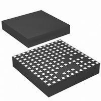
IC BUCK SYNC ADJ 5A 133LGA
Manufacturer
Linear Technology
Series
µModuler
Type
Point of Load (POL) Non-Isolatedr
Datasheet
1.LTM4612EVPBF.pdf
(26 pages)
Specifications of LTM4612MPV#PBF
Design Resources
LTM4612 Spice Model
Output
3.3 ~ 15 V
Number Of Outputs
1
Power (watts)
75W
Mounting Type
Surface Mount
Voltage - Input
5 ~ 36 V
Package / Case
133-LGA
1st Output
3.3 ~ 15 VDC @ 5A
Size / Dimension
0.59" L x 0.59" W x 0.11" H (15mm x 15mm x 2.8mm)
Power (watts) - Rated
75W
Operating Temperature
-55°C ~ 125°C
Lead Free Status / RoHS Status
Lead free / RoHS Compliant
3rd Output
-
2nd Output
-
Available stocks
Company
Part Number
Manufacturer
Quantity
Price


operaTion
LTM4612
Power Module Description
The LTM4612 is a standalone nonisolated switching mode
DC/DC power supply. It can deliver 5A of DC output
current with some external input and output capacitors.
This module provides precisely regulated output voltage
programmable via one external resistor from 3.3V
15V
application schematic is shown in Figure 18.
The LTM4612 has an integrated constant on-time current
mode regulator, ultralow R
speed and integrated Schottky diodes. The typical switching
frequency is 850kHz at full load at 12V output. With current
mode control and internal feedback loop compensation,
the LTM4612 module has sufficient stability margins and
good transient performance under a wide range of operat-
ing conditions and with a wide range of output capacitors,
even all ceramic output capacitors.
Current mode control provides cycle-by-cycle fast current
limiting. Moreover, foldback current limiting is provided in
an overcurrent condition while V
voltage and undervoltage comparators pull the open-drain
PGOOD output low if the output feedback voltage exits a
±10% window around the regulation point. Furthermore,
in an overvoltage condition, internal top FET M1 is turned
off and bottom FET M2 is turned on and held on until the
overvoltage condition clears.
0
DC
over a 5V to 36V wide input voltage. The typical
DS(ON)
FETs with fast switching
FB
drops. Internal over-
DC
to
Input filter and noise cancellation circuitry reduce the
noise coupling to I/O sides, and ensure the electromag-
netic interference (EMI) meets the limits of CISPR 22 and
CISPR 25.
Pulling the RUN pin below 1V forces the controller into its
shutdown state, turning off both M1 and M2. At low load
currents, discontinuous mode (DCM) operation can be
enabled to achieve higher efficiency compared to continu-
ous mode (CCM) by setting FCB pin higher than 0.6V.
When the DRV
5V linear regulator powers the internal gate drivers. If a
5V external bias supply is applied on DRV
efficiency improvement will occur due to the reduced power
loss in the internal linear regulator. This is especially true
at the higher input voltage range.
The MPGM, MARG0, and MARG1 pins are used to sup-
port voltage margining, where the percentage of margin
is programmed by the MPGM pin, and the MARG0 and
MARG1 selected margining. The PLLIN pin provides fre-
quency synchronization of the device to an external clock.
The TRACK/SS pin is used for power supply tracking and
soft-start programming.
CC
pin is connected to INTV
CC
CC
, an integrated
pin, then an
4612fa
Related parts for LTM4612MPV#PBF
Image
Part Number
Description
Manufacturer
Datasheet
Request
R

Part Number:
Description:
CD ROM LINEARVIEW DATASHEETS
Manufacturer:
Linear Technology

Part Number:
Description:
Standalone Linear Li-Ion Battery Charger with Thermal Regulation in ThinSOT
Manufacturer:
Linear Technology Corporation
Datasheet:
Part Number:
Description:
Low noise, high frequency, 8th order linear phase lowpass filter
Manufacturer:
Linear Technology Corporation
Datasheet:
Part Number:
Description:
Manufacturer:
Linear Technology Corporation
Datasheet:
Part Number:
Description:
Manufacturer:
Linear Technology Corporation
Datasheet:
Part Number:
Description:
Manufacturer:
Linear Technology Corporation
Datasheet:
Part Number:
Description:
Manufacturer:
Linear Technology Corporation
Datasheet:
Part Number:
Description:
Manufacturer:
Linear Technology Corporation
Datasheet:
Part Number:
Description:
Manufacturer:
Linear Technology Corporation
Datasheet:
Part Number:
Description:
Manufacturer:
Linear Technology Corporation
Datasheet:
Part Number:
Description:
Dual and Quad, JFET Input Precision High Speed Op Amps
Manufacturer:
Linear Technology Corporation
Datasheet:
Part Number:
Description:
Manufacturer:
Linear Technology Corporation
Datasheet:
Part Number:
Description:
1, 2, 6 and 8 Channel, 10-Bit Serial I/O Data Acquisition Systems
Manufacturer:
Linear Technology Corporation
Datasheet:
Part Number:
Description:
Manufacturer:
Linear Technology Corporation
Datasheet:
Part Number:
Description:
Universal dual filter building block
Manufacturer:
Linear Technology Corporation
Datasheet: