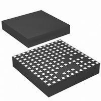
LTM4612MPV#PBF Linear Technology, LTM4612MPV#PBF Datasheet - Page 15

LTM4612MPV#PBF
Manufacturer Part Number
LTM4612MPV#PBF
Description
IC BUCK SYNC ADJ 5A 133LGA
Manufacturer
Linear Technology
Series
µModuler
Type
Point of Load (POL) Non-Isolatedr
Datasheet
1.LTM4612EVPBF.pdf
(26 pages)
Specifications of LTM4612MPV#PBF
Design Resources
LTM4612 Spice Model
Output
3.3 ~ 15 V
Number Of Outputs
1
Power (watts)
75W
Mounting Type
Surface Mount
Voltage - Input
5 ~ 36 V
Package / Case
133-LGA
1st Output
3.3 ~ 15 VDC @ 5A
Size / Dimension
0.59" L x 0.59" W x 0.11" H (15mm x 15mm x 2.8mm)
Power (watts) - Rated
75W
Operating Temperature
-55°C ~ 125°C
Lead Free Status / RoHS Status
Lead free / RoHS Compliant
3rd Output
-
2nd Output
-
Available stocks
Company
Part Number
Manufacturer
Quantity
Price
applicaTions inForMaTion
COMP Pin
The pin is the external compensation pin. The module
has already been internally compensated for most output
voltages. An Excel design tool from Linear Technology will
be provided for more control loop optimization.
FCB Pin
The FCB pin determines whether the bottom MOSFET
remains on when current reverses in the inductor. Tying
this pin above its 0.6V threshold enables discontinuous
operation where the bottom MOSFET turns off when in-
ductor current reverses. FCB pin below the 0.6V threshold
forces continuous synchronous operation, allowing current
to reverse at light loads and maintaining high frequency
operation.
PLLIN Pin
The power module has a phase-locked loop comprised
of an internal voltage controlled oscillator and a phase
detector. This allows the internal top MOSFET turn-on
to be locked to the rising edge of the external clock.
The frequency range is ±30% around the set operating
frequency. A pulse detection circuit is used to detect a
clock on the PLLIN pin to turn on the phase-locked loop.
The pulse width of the clock has to be at least 400ns, and
2V in amplitude. During the start-up of the regulator, the
phase-locked loop function is disabled.
INTV
An internal low dropout regulator produces an internal
5V supply that powers the control circuitry and DRV
for driving the internal power MOSFETs. Therefore, if
the system does not have a 5V power rail, the LTM4612
can be directly powered by V
through the LDO is about 20mA. The internal LDO power
dissipation can be calculated as:
The LTM4612 also provides the external gate driver voltage
pin DRV
mended to connect the DRV
This is especially true for higher input voltages. Do not
apply more than 6V to the DRV
P
LDO_LOSS
CC
and DRV
CC
. If there is a 5V rail in the system, it is recom-
= 20mA • (V
CC
Connection
IN
CC
– 5V)
IN
pin to the external 5V rail.
CC
. The gate driver current
pin.
CC
Parallel Operation
The LTM4612 device is an inherently current mode con-
trolled device. This allows the paralleled modules to have
very good current sharing and balanced thermal on the
design. Figure 21 shows a schematic of the parallel design.
The voltage feedback equation changes with the variable
N as modules are paralleled. The equation:
N is the number of paralleled modules.
Radiated EMI Noise
High radiated EMI noise is a disadvantage for switching
regulators by nature. Fast switching turn-on and turn-off
make the large di/dt change in the converters, which act
as the radiation sources in most systems. LTM4612 inte-
grates the feature to minimize the radiated EMI noise to
meet the most applications with low noise requirements.
An optimized gate driver for the MOSFET and a noise
cancellation network are installed inside the LTM4612
to achieve the low radiated EMI noise. Figure 8 shows a
typical example for the LTM4612 to meet the Class B of
CISPR 22 radiated emission limit.
Thermal Considerations and Output Current Derating
In different applications, LTM4612 operates in a variety
of thermal environments. The maximum output current is
limited by the environment thermal condition. Sufficient
cooling should be provided to help ensure reliable opera-
V
OUT
Figure 8. Radiated Emission Scan with 24V
12V
=
90
70
50
30
10
OUT
0
0 6
0
.
at 5A Measured in 10 Meter Chamber
100
V
100
200
N
R
k
300
FB
+
FREQUENCY (MHz)
R
400
FB
CISPR22, CLASS B
500
600
700
800
LTM4612
900
4612 F08
IN
1000
to
4612fa


