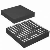
LTM4612MPV#PBF Linear Technology, LTM4612MPV#PBF Datasheet - Page 12

LTM4612MPV#PBF
Manufacturer Part Number
LTM4612MPV#PBF
Description
IC BUCK SYNC ADJ 5A 133LGA
Manufacturer
Linear Technology
Series
µModuler
Type
Point of Load (POL) Non-Isolatedr
Datasheet
1.LTM4612EVPBF.pdf
(26 pages)
Specifications of LTM4612MPV#PBF
Design Resources
LTM4612 Spice Model
Output
3.3 ~ 15 V
Number Of Outputs
1
Power (watts)
75W
Mounting Type
Surface Mount
Voltage - Input
5 ~ 36 V
Package / Case
133-LGA
1st Output
3.3 ~ 15 VDC @ 5A
Size / Dimension
0.59" L x 0.59" W x 0.11" H (15mm x 15mm x 2.8mm)
Power (watts) - Rated
75W
Operating Temperature
-55°C ~ 125°C
Lead Free Status / RoHS Status
Lead free / RoHS Compliant
3rd Output
-
2nd Output
-
Available stocks
Company
Part Number
Manufacturer
Quantity
Price
LTM4612
applicaTions inForMaTion
If lower output ripple is required, the operating frequency
f can be increased by adding a resistor R
pin and SGND, as shown in Figure 19.
For output voltages more than 12V, the frequency can be
higher than 1MHz, thus reducing the efficiency significantly.
Additionally, the minimum off time 400ns normally limits
the operation when the input voltage is close to the output
voltage. Therefore, it is recommended to lower the fre-
quency in these conditions by connecting a resistor (R
from the f
The load current can affect the frequency due to its constant
on-time control. If constant frequency is a necessity, the
PLLIN pin can be used to synchronize the frequency of
the LTM4612 to an external clock, as shown in Figures
21 to 23.
Input Capacitors
LTM4612 is designed to achieve the low input conducted
EMI noise due to the fast switching of turn-on and turn-off.
In the LTM4612, a high-frequency inductor is integrated
into the input line for noise attenuation. V
are available for external input capacitors to form a high
frequency π filter. As shown in Figure 18, the ceramic
capacitor C1 on the V
the RMS current into the converter, so careful attention
is needed for capacitor C1 selection.
For a buck converter, the switching duty cycle can be
estimated as:
Without considering the inductor current ripple, the RMS
current of the input capacitor can be estimated as:
D
I
f
f
CIN RMS
=
=
=
(
1 5 10
5 10
V
V
. •
OUT
•
IN
SET
)
=
−
pin to V
11
I
OUT MAX
−
10
R
(
V
3
h
(
V
OUT
R
fSET
•
OUT
IN
R
fSET
D
)
, as shown in Figure 20.
fSET
pins is used to handle most of
•
−
||
2 93 1
D
•
93 1
•
93 1
• –
(
.
1
.
.
k
k
)
k
D
)
fSET
D
between f
and V
IN
fSET
pins
SET
)
In this equation, h is the estimated efficiency of the
power module. Note the capacitor ripple current ratings
are often based on temperature and hours of life. This
makes it advisable to properly derate the input capacitor,
or choose a capacitor rated at a higher temperature than
required. Always contact the capacitor manufacturer for
derating requirements.
In a typical 5A output application, one very low ESR, X5R
or X7R, 10µF ceramic capacitor is recommended for C1.
This decoupling capacitor should be placed directly adja-
cent to the module V
the trace inductance and high frequency AC noise. Each
10µF ceramic is typically good for 2A to 3A of RMS ripple
current. Refer to your ceramics capacitor catalog for the
RMS current ratings.
To attenuate the high frequency noise, extra input capacitors
should be connected to the V
high frequency inductor to form the π filter. One of these
low ESR ceramic input capacitors is recommended to be
close to the connection into the system board. A large
bulk 100µF capacitor is only needed if the input source
impedance is compromised by long inductive leads or
traces. Figure 4 shows the conducted EMI testing results
to meet the Level 5 of the CISPR 25 limit. For different
applications, input capacitance may be varied to meet
different conducted EMI limits.
80
70
60
50
40
30
20
10
Figure 4. Conducted Emission Scan with 24V
12V
Pads and 1
0
0.15
CIS25QP
OUT
at 5A (3
×
10µF Ceramic Capacitor on V
D
×
10µF Ceramic Capacitors on V
pins in the PCB layout to minimize
1
FREQUENCY (MHz)
IN
pads and placed before the
10
D
Pads).
IN
4612 F04
to
IN
30
4612fa


