HSC-ADC-EVALCZ Analog Devices Inc, HSC-ADC-EVALCZ Datasheet - Page 8
HSC-ADC-EVALCZ
Manufacturer Part Number
HSC-ADC-EVALCZ
Description
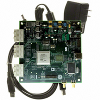
KIT EVAL ADC FIFO HI SPEED
Manufacturer
Analog Devices Inc
Datasheets
1.HSC-ADC-EVALB-DCZ.pdf
(28 pages)
2.HSC-ADC-EVALCZ.pdf
(32 pages)
3.HSC-ADC-EVALCZ.pdf
(40 pages)
Specifications of HSC-ADC-EVALCZ
Design Resources
EVALC PC Board Gerber File
Accessory Type
ADC Interface Board
Silicon Manufacturer
Analog Devices
Application Sub Type
ADC
Kit Application Type
Data Converter
Features
Buffer Memory Board For Capturing Digital Data, USB Port Interface, Windows 98, Windows 2000
Kit Contents
ADC Analyzer, Buffer Memory Board
Rohs Compliant
Yes
Lead Free Status / RoHS Status
Lead free / RoHS Compliant
For Use With/related Products
Single ADC Version
Lead Free Status / Rohs Status
Supplier Unconfirmed
Available stocks
Company
Part Number
Manufacturer
Quantity
Price
Company:

Part Number:
HSC-ADC-EVALCZ
Manufacturer:
Analog Devices Inc
Quantity:
135


HSC-ADC-EVALC
THEORY OF OPERATION
The HSC-ADC-EVALC evaluation platform is based around
the Virtex-4 FPGA (XC4VFX20-10FFG672C) from Xilinx®,
which can be programmed through VisualAnalog to operate
with a variety of data converters. Another key component, the
Cypress USB device (U3), communicates with a host PC and
provides the SPI interface used for configuration.
CONFIGURATION
Some converter devices require programming for mode or
feature selection, which the SPI controller accomplishes using
SPI-accessible register maps. U3 drives the 4-wire SPI (SCLK,
SDI, SDO, CSB
(J1). For more information on serial port interface (SPI) func-
tions, consult the user manual titled Interfacing to High Speed
ADCs via SPI at www.analog.com/FIFO.
The SPI interface designed on the Cypress IC can communicate
with up to five different SPI-enabled devices including the
FPGA. The CLK and SDI/SDO data lines are common to all SPI
devices. The desired SPI-enabled device is selected for control
by using one of the five active low chip select (CS) pins. This
functionality is controlled by selecting a SPI channel in the SPI
Controller software.
At power-up, VisualAnalog attempts to autodetect the converter
that is attached to the ADC capture board using the SPI
interface. If a recognized device is found, VisualAnalog selects
the appropriate FPGA configuration; otherwise, the user is
prompted to make the device selection. In either case,
VisualAnalog then programs the FPGA using the SPI interface
of U3. The configurations typically program a FIFO data capture
function within the FPGA.
INPUT CIRCUITRY
The parallel data input pins of the FPGA, which interface to the
converter, are configurable. They can operate with 1.8 V, 2.5 V,
or 3.3 V logic levels and can accept LVDS or CMOS inputs.
Each channel of the ADC capture board requires a clock signal
to capture data. These clock signals are normally provided by
the attached ADC evaluation board and are passed along with
the data through one or more pins on Connector J2 and/or
1
) signals to the converter board via connector
Rev. 0 | Page 8 of 32
Connector J3. Refer to the HSC-ADC-EVALC I/O connector
pin mappings shown in Figure 21 and Figure 22.
DATA CAPTURE
The process of filling the FIFO and reading the data back
requires several steps.
1.
2.
3.
4.
CODE DESCRIPTION
FPGA configuration files are provided by ADI for all ADCs
supported by the HSC-ADC-EVALC evaluation platform.
These files are designed and tested to facilitate quick
performance evaluations of Analog Devices data converters. No
additional FPGA programming is required from the user for
typical operation.
FPGA CONFIGURATION AND CUSTOMIZATION
Users can manually customize or update the FPGA code
through a JTAG connector (J10) provided on the ADC capture
board, as shown in Figure 17. However, Analog Devices
provides no support or guarantee of performance if the
provided code is customized by the user.
The HSC-ADC-EVALC hardware platform may contain addi-
tional circuit functions to support future developments and
capabilities. These functions are not supported beyond the
scope of this data sheet and the Analog Devices supplied data-
capture FPGA routines at this time.
Additional FPGA programming support may be available
through the user’s local Xilinx representative or distributor.
1
Note that CSB1 is the default CSB line used.
VisualAnalog initiates the FIFO fill process by resetting
the FIFOs.
The 48 MHz USB read clock (RCLK) is then suspended to
ensure that it does not add noise to the ADC input.
VisualAnalog waits approximately 30 ms to allow for data
capture before beginning the readback process. This wait
time is an adjustable parameter in VisualAnalog.
VisualAnalog reads the data from the FIFO through the
USB interface to the PC.
Related parts for HSC-ADC-EVALCZ
Image
Part Number
Description
Manufacturer
Datasheet
Request
R

Part Number:
Description:
KIT EVAL ADC FIFO DUAL-CH USB HS
Manufacturer:
Analog Devices Inc
Datasheet:

Part Number:
Description:
KIT EVAL ADC USB FIFO HI-SPEED
Manufacturer:
Analog Devices Inc
Datasheet:

Part Number:
Description:
BOARD FPGA OCTAL LVDS FOR ADC
Manufacturer:
Analog Devices Inc
Datasheet:
Part Number:
Description:
KIT EVAL FOR SINGLE CHAN HSC ADC
Manufacturer:
Analog Devices Inc

Part Number:
Description:
KIT EVAL FOR DUAL ADC/CONV
Manufacturer:
Analog Devices Inc
Datasheet:
Part Number:
Description:
KIT EVAL ADC USB FIFO HI-SPEED
Manufacturer:
Analog Devices Inc
Datasheet:

Part Number:
Description:
KIT EVAL ADC USB FIFO HI-SPEED
Manufacturer:
Analog Devices Inc
Datasheet:
Part Number:
Description:
KIT EVAL ADC FIFO DUAL-CH USB HS
Manufacturer:
Analog Devices Inc
Datasheet:
Part Number:
Description:
BOARD FPGA QUAD LVDS FOR ADC
Manufacturer:
Analog Devices Inc
Datasheet:
Part Number:
Description:
Adapter For AD922x Family
Manufacturer:
Analog Devices Inc
Datasheet:
Part Number:
Description:
Interposer Quad/octal ADCs
Manufacturer:
Analog Devices Inc
Datasheet:

Part Number:
Description:
±1.7g Dual-Axis IMEMS Accelerometer Evaluation Board
Manufacturer:
Analog Devices Inc
Datasheet:

Part Number:
Description:
IC MULTIPLIER ANALOG 8-SOIC T/R
Manufacturer:
Analog Devices Inc
Datasheet:
Part Number:
Description:
IC ANALOG MULTIPLIER 8-DIP
Manufacturer:
Analog Devices Inc
Datasheet: