DLP-2232M-G DLP Design Inc, DLP-2232M-G Datasheet - Page 28
DLP-2232M-G
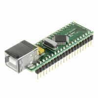
Manufacturer Part Number
DLP-2232M-G
Description
MODULE USB ADAPTER FOR FT2232D
Manufacturer
DLP Design Inc
Datasheet
1.DLP-2232M-G.pdf
(33 pages)
Specifications of DLP-2232M-G
Main Purpose
Interface, USB 2.0 to UART (RS232) Bridge
Embedded
No
Utilized Ic / Part
FT2232D
Primary Attributes
Full Speed USB to High-Speed UART
Secondary Attributes
Royalty-Free Drivers, 2K EEPROM
Interface Type
USB
Data Bus Width
8 bit
Operating Supply Voltage
4.35 V to 5.25 V
Product
Interface Modules
For Use With/related Products
FT2232D
Lead Free Status / RoHS Status
Lead free / RoHS Compliant
Lead Free Status / RoHS Status
Lead free / RoHS Compliant, Lead free / RoHS Compliant
Other names
813-1000


Figure 30 - MCU Host Bus Emulation Mode Signal Timing - Read Cycle
Time
t1
t2
t3
t4
t5
t6
t7
t8
t9
Figure 31 - MCU Host Bus Emulation Mode Signal Timing - Clock (OSC) Signal
Rev 1.6 (May 2009)
A15..A8
AD7..0
IORDY
ALE
CS#
OSC
RD#
OSC
Time
tperiod
Description
High address byte is placed on the bus if the extended read is used - otherwise
t1 will not occur.
Low address byte is put out.
1 clock period for address set up.
ALE goes high to enable address latch. This will extend to 2 clocks wide if
IORDY# is low.
ALE goes low to latch address, and CS# is set active low. This will extend to 3
clocks if IORDY# is sam-pled low. CS# will always drop 1 clock after ALE has
gone high no matter the state of IORDY#.
Data is set as input (Hi-Z), and RD# is driven active low.
1 clock period for data setup. This will extend to 5 clocks wide if IORDY# is
sampled low.
RD# is driven inactive high.
CS# is driven inactive 1/2 a clock period after RD# goes inactive, and the data
bus is set back to output.
t
high
t1
Description
Clock Period
t2
t
low
High Address
t3
Low Address
t4
t
28
period
t5
Typical
Value
??
DLP-2232M-G DLP Design, Inc.
t6
Hi-Z
t7
Unit
ns
t8 t9
Related parts for DLP-2232M-G
Image
Part Number
Description
Manufacturer
Datasheet
Request
R

Part Number:
Description:
MODULE USB-TO-TTL PARL FIFO CONV
Manufacturer:
DLP Design Inc
Datasheet:

Part Number:
Description:
KIT DEV DLP LIGHTCOMANDER
Manufacturer:
Logic
Datasheet:

Part Number:
Description:
MODULE DATA-ACQUISITION 8-CH
Manufacturer:
DLP Design Inc
Datasheet:

Part Number:
Description:
MODULE DATA-ACQUISITION 20-CH
Manufacturer:
DLP Design Inc
Datasheet:

Part Number:
Description:
RFID READER/WRITER SNGL-CH OEM
Manufacturer:
DLP Design Inc
Datasheet:

Part Number:
Description:
Interface Modules & Development Tools DLP-245PL PACKAGED w/CCS Compiler
Manufacturer:
DLP Design Inc

Part Number:
Description:
Interface Modules & Development Tools DLP-245PB-G BOARD + CCS Compiler
Manufacturer:
DLP Design Inc
Datasheet:

Part Number:
Description:
Interface Modules & Development Tools DLP-TILT SENSOR ACCEL VIBRATION
Manufacturer:
DLP Design Inc

Part Number:
Description:
MODULE USB-MCU FT245RL W/16F877A
Manufacturer:
DLP Design Inc
Datasheet:

Part Number:
Description:
MODULE USB-TO-FPGA TRAINING TOOL
Manufacturer:
DLP Design Inc
Datasheet:

Part Number:
Description:
MODULE USB-MCU FT232R W/18F2410
Manufacturer:
DLP Design Inc
Datasheet:

Part Number:
Description:
MODULE USB-MCU FT245RL W/SX48
Manufacturer:
DLP Design Inc
Datasheet:

Part Number:
Description:
MODULE USB-MCU FT2232D W/16F877A
Manufacturer:
DLP Design Inc
Datasheet:

Part Number:
Description:
MODULE USB-TO-FPGA SPARTAN3
Manufacturer:
DLP Design Inc
Datasheet:

Part Number:
Description:
MOD USB-MCU FT245RL W/18LF8722
Manufacturer:
DLP Design Inc
Datasheet: