OM6281 NXP Semiconductors, OM6281 Datasheet - Page 10
OM6281
Manufacturer Part Number
OM6281
Description
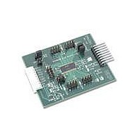
DAUGHTER CARD PCA9698 FOR OM6275
Manufacturer
NXP Semiconductors
Datasheet
1.OM6281.pdf
(16 pages)
Specifications of OM6281
Main Purpose
Interface, GPIO Expander
Embedded
No
Utilized Ic / Part
OM6275, PCA9698
Primary Attributes
40-Bit 40-Port GPIO Expander
Secondary Attributes
I²C Interface
Interface Type
I2C
For Use With/related Products
PCA9698
Lead Free Status / RoHS Status
Lead free / RoHS Compliant
Lead Free Status / RoHS Status
Lead free / RoHS Compliant, Lead free / RoHS Compliant
Available stocks
Company
Part Number
Manufacturer
Quantity
Price
Company:

Part Number:
OM6281
Manufacturer:
NXP Semiconductors
Quantity:
135


NXP Semiconductors
9. Application specific: LED blinking and dimming with the PCA9530 and
UM10267_1
User manual
the PCA9698
8.2.1 Polling mode
8.2.2 Interrupt mode
8.2 GPIO input
9.1 Theory of operation
In polling mode, the host controller must read the input port registers at predetermined
intervals to check if an input has changed. Depending on the application, the interrupt
mode described in
state on the input pins.
In interrupt mode the interrupt pin is toggled to signal the host controller when an input
change of state has been detected. The interrupt mask register specifies which signal is
allowed to generate an interrupt.
The PCA9698 has the capability to drive up to 40 LEDs (within certain power restrictions
on the package, which can be overcome with the use of FETs). To enhance the
application of the PCA9698, a PCA9530 can be used to drive the Output Enable (OE) pin
to blink and dim the output of the LEDs. A pattern with intermediate complexity can be
easily generated by combining the outputs of the PCA9530.
A 74LVC1G38GW NAND gate is used to demonstrate the OE polarity inversion (active
HIGH instead of default active LOW) of the PCA9698.
1. Select Bank0 and verify that the default values are displayed.
2. Since the PCA9698 has a small pull-up on the I/O, a read on the Input Port 0 register
3. Pull Port0.7 to a logic LOW.
4. Read the Input Port 0 register and verify that the Input Port 0 register reads 0x7F.
1. Select Bank1 and verify the default values are active.
2. Un-check the MSK7 and MSK6 bits in the Mask Interrupt 1 register.
3. With the aid of an external pull-down, pull Port1.6 and Port1.7 bits to a logic LOW.
4. Verify the INT light is illuminated on the board.
5. Toggle the MSK6 and MSK7 bits and verify the INT light goes off only when both bits
6. Read the Input Port 1 register and verify the contents is now 0x3F and the INT light is
7. Pull the IO1.7 signal HIGH and verify that the interrupt light is on.
8. Toggle the MSK6 bit and verify that the INT light remains on.
9. Read the Input Port 1 register and verify that the contents is 0xBF and the INT light is
returns 0xFF.
are masked.
off.
off.
Section 8.2.2
Rev. 01 — 24 September 2008
may be a more efficient method of verifying changes of
PCA9698 demonstration board OM6281
UM10267
© NXP B.V. 2008. All rights reserved.
10 of 16
Related parts for OM6281
Image
Part Number
Description
Manufacturer
Datasheet
Request
R

Part Number:
Description:
NXP Semiconductors designed the LPC2420/2460 microcontroller around a 16-bit/32-bitARM7TDMI-S CPU core with real-time debug interfaces that include both JTAG andembedded trace
Manufacturer:
NXP Semiconductors
Datasheet:

Part Number:
Description:
NXP Semiconductors designed the LPC2458 microcontroller around a 16-bit/32-bitARM7TDMI-S CPU core with real-time debug interfaces that include both JTAG andembedded trace
Manufacturer:
NXP Semiconductors
Datasheet:
Part Number:
Description:
NXP Semiconductors designed the LPC2468 microcontroller around a 16-bit/32-bitARM7TDMI-S CPU core with real-time debug interfaces that include both JTAG andembedded trace
Manufacturer:
NXP Semiconductors
Datasheet:
Part Number:
Description:
NXP Semiconductors designed the LPC2470 microcontroller, powered by theARM7TDMI-S core, to be a highly integrated microcontroller for a wide range ofapplications that require advanced communications and high quality graphic displays
Manufacturer:
NXP Semiconductors
Datasheet:
Part Number:
Description:
NXP Semiconductors designed the LPC2478 microcontroller, powered by theARM7TDMI-S core, to be a highly integrated microcontroller for a wide range ofapplications that require advanced communications and high quality graphic displays
Manufacturer:
NXP Semiconductors
Datasheet:
Part Number:
Description:
The Philips Semiconductors XA (eXtended Architecture) family of 16-bit single-chip microcontrollers is powerful enough to easily handle the requirements of high performance embedded applications, yet inexpensive enough to compete in the market for hi
Manufacturer:
NXP Semiconductors
Datasheet:
Part Number:
Description:
The XA-S3 device is a member of Philips Semiconductors? XA(eXtended Architecture) family of high performance 16-bitsingle-chip microcontrollers
Manufacturer:
NXP Semiconductors
Datasheet:

Part Number:
Description:
The NXP BlueStreak LH75401/LH75411 family consists of two low-cost 16/32-bit System-on-Chip (SoC) devices
Manufacturer:
NXP Semiconductors
Datasheet:
Part Number:
Description:
The NXP LPC3130/3131 combine an 180 MHz ARM926EJ-S CPU core, high-speed USB2
Manufacturer:
NXP Semiconductors
Datasheet:
Part Number:
Description:
The NXP LPC3141 combine a 270 MHz ARM926EJ-S CPU core, High-speed USB 2
Manufacturer:
NXP Semiconductors
Part Number:
Description:
The NXP LPC3143 combine a 270 MHz ARM926EJ-S CPU core, High-speed USB 2
Manufacturer:
NXP Semiconductors

Part Number:
Description:
The NXP LPC3152 combines an 180 MHz ARM926EJ-S CPU core, High-speed USB 2
Manufacturer:
NXP Semiconductors
Part Number:
Description:
The NXP LPC3154 combines an 180 MHz ARM926EJ-S CPU core, High-speed USB 2
Manufacturer:
NXP Semiconductors

Part Number:
Description:
Standard level N-channel enhancement mode Field-Effect Transistor (FET) in a plastic package using NXP High-Performance Automotive (HPA) TrenchMOS technology
Manufacturer:
NXP Semiconductors
Datasheet: