ADV212-HD-EB Analog Devices Inc, ADV212-HD-EB Datasheet - Page 24
ADV212-HD-EB
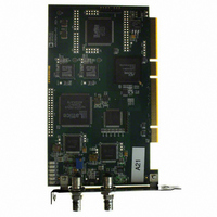
Manufacturer Part Number
ADV212-HD-EB
Description
BOARD EVALUATION FOR ADV212-HD
Manufacturer
Analog Devices Inc
Datasheet
1.ADV212BBCZRL-115.pdf
(44 pages)
Specifications of ADV212-HD-EB
Main Purpose
Video, Video Processing
Embedded
Yes, FPGA / CPLD
Utilized Ic / Part
ADV212-HD
Primary Attributes
1080i and 720p SDI Compatible, 32/64-bit, 33/66 MHz PCI Card
Secondary Attributes
GUI, JPEG2000 Video Codec
Lead Free Status / RoHS Status
Contains lead / RoHS non-compliant


ADV212
Pin No.
1, 4, 9,11,
23, 33, 39,
45, 49 to
51, 55, 56,
60 to 62,
66, 67, 71
to 73, 77,
83, 89, 99,
110, 111,
118, 121
17, 28, 30,
38, 52, 74,
82, 93, 104
to 106
1
2
3
In fly-by mode DMA, the functions of the RD and WE signals (for DMA only) are reversed. This allows a host to move data between an external device and the ADV212
with the use of a single strobe.
In encode mode with fly-by DMA, the host can use the RDFB signal ( WE pin) to simultaneously read from the ADV212 and write to an external device such as memory.
In decode mode with fly-by DMA, the host can use the WEFB signal ( RD pin) to simultaneously read from the external device and write to the ADV212.
121-Ball Package
Location
A1, A4, A9,
A11, C1,
C11, D6, E1,
E5 to E7,
E11, F1, F5
to F7, F11,
G1, G5 to
G7, G11,
H6, J1, J11,
K11, L1, L8,
L11
B6, C6, C8,
D5, E8, G8,
H5, J5, K5
to K7
Pin No.
1, 5 to 8, 12,
17, 20, 29,
32, 41, 44,
52 to 56, 65
to 68, 77 to
81, 89 to
93, 101,
104, 105,
113, 116,
125, 128,
133, 137 to
140, 143,
144
16, 21, 28,
33, 40, 45,
112, 117,
124, 129
144-Ball Package
Location
A1, A5 to
A8, A12, B5,
B8, C5, C8,
D5, D8, E4
to E8, F5 to
F8, G5 to
G9, H5 to
H9, J5, J8,
J9, K5, K8,
L5, L8, M1,
M5 to M8,
M11, M12
B4, B9, C4,
C9, D4, D9,
K4, K9, L4,
L9
Mnemonic
DGND
IOVDD
Rev. B | Page 24 of 44
Pins
Used
29/45
11/10
Type
GND
V
Description
Ground.
Positive Supply for Input/Output.
Related parts for ADV212-HD-EB
Image
Part Number
Description
Manufacturer
Datasheet
Request
R

Part Number:
Description:
BOARD EVAL FOR ADV212 CODEC
Manufacturer:
Analog Devices Inc
Datasheet:

Part Number:
Description:
±1.7g Dual-Axis IMEMS Accelerometer Evaluation Board
Manufacturer:
Analog Devices Inc
Datasheet:
Part Number:
Description:
Inertial Sensor Evaluation System
Manufacturer:
Analog Devices Inc
Datasheet:
Part Number:
Description:
Manufacturer:
Analog Devices Inc
Datasheet:
Part Number:
Description:
Manufacturer:
Analog Devices Inc
Datasheet:
Part Number:
Description:
Manufacturer:
Analog Devices Inc
Datasheet:
Part Number:
Description:
Manufacturer:
Analog Devices Inc
Datasheet:
Part Number:
Description:
Manufacturer:
Analog Devices Inc
Datasheet:
Part Number:
Description:
Manufacturer:
Analog Devices Inc
Datasheet:
Part Number:
Description:
Manufacturer:
Analog Devices Inc
Datasheet:
Part Number:
Description:
Manufacturer:
Analog Devices Inc
Datasheet:
Part Number:
Description:
Manufacturer:
Analog Devices Inc
Datasheet:
Part Number:
Description:
Manufacturer:
Analog Devices Inc
Datasheet: