M3A-0033 Renesas Electronics America, M3A-0033 Datasheet - Page 22
M3A-0033
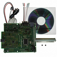
Manufacturer Part Number
M3A-0033
Description
DEV EVALUATION BOARD FOR M66291G
Manufacturer
Renesas Electronics America
Datasheet
1.M3A-0033.pdf
(39 pages)
Specifications of M3A-0033
Main Purpose
USB Controller
Embedded
*
Utilized Ic / Part
M66291
Primary Attributes
*
Secondary Attributes
*
Lead Free Status / RoHS Status
Contains lead / RoHS non-compliant


Chapter8. M3A-0033 Specification
8.1 Block Diagram
M66291GP Evaluation Board
Note: When M3A-0029B is connected, the signal lines marked
The block diagram of M3A-0033 is shown in Figure 8-1.
application
M3A-0029B
mounted
M3A-0032
Board
6629x
board
External
Power supply
User
5.0V
or
Vbus
Dreq0
INT1,SOF
P6[0:5],P7 [0:7] ,P80,P81,P85,P86, P87,P9[0:7],P10[0:7]
INT0
(3.3V)
TC1
Dreq1
For Dack 0
For Dack 1
CS0,CS1,CS2
CS3(only mode3)
/
Reg1
A[0:6]
RD,WRL,WRH
A[0:19]
U5
CS
D[0:15]
UART0
HOLD
EXIOVcc
RD,WRL,WRH
RDY
EX_Vcc
D[0:15]
BCLK,HLDA,ALE
RST
U6 not mounted
JP15
JP14
JP7 short-circuit
JP18
JP9
(3.3V) U6
Reg2
5.0V
JP5
3.3V
Figure 8-1 M3A-0033 System Block Diagram
JP17
Clock circuit
10MHz
3.3V
VCC
GND
JP6
JP16
- 18 -
INT1(for Dreq0)
JP2
INT2
INT0
P106
P107
CS 1
CS2
CS3
JP8 short-circuit
for reset
circuit
Delay
JP11
3.3V
Xout
CNVss
Xin
M16C/80
RXD0(36)
CTS0(38)
U1
TXD0(35)
P70
TxD1(31)
RXD1(32)
BYTE
HOLD
P80(22)
CLK1
JP1
3
2
4
UART1
JP12
JP20
for reset
JP4
circuit
Delay
JP3
are invalid.
SW2
2 circuits
VCC
JP13
JP21
GND
GND
(RxD1,TxD1)
GND
GND
MAX
3241
U5
VCC
GND
SW3
VCC
1
/RESET
Vcc of M16C/80
SW1
UART0
UART1
VCC
RTS
RD
CTS
RD
TD
TD
Modular
socket
4pin
RS232C
debugger
M3A-0033
PC
PC for
Related parts for M3A-0033
Image
Part Number
Description
Manufacturer
Datasheet
Request
R

Part Number:
Description:
DEV EVALUATION BOARD FOR M66592
Manufacturer:
Renesas Electronics America
Part Number:
Description:
DEV EVALUATION KIT FOR M66596
Manufacturer:
Renesas Electronics America
Datasheet:
Part Number:
Description:
DEV EVALUATION BOARD FOR M66591G
Manufacturer:
Renesas Electronics America
Part Number:
Description:
M35054/M35055-XXXSP/FP EVAL BOAR
Manufacturer:
Renesas Electronics America
Part Number:
Description:
DEV M35070/71-XXXFP,M35047-XXXFP
Manufacturer:
Renesas Electronics America
Part Number:
Description:
DEV EVALUATION BOARD 38K0/38K2 G
Manufacturer:
Renesas Electronics America

Part Number:
Description:
KIT STARTER FOR M16C/29
Manufacturer:
Renesas Electronics America
Datasheet:

Part Number:
Description:
KIT STARTER FOR R8C/2D
Manufacturer:
Renesas Electronics America
Datasheet:

Part Number:
Description:
R0K33062P STARTER KIT
Manufacturer:
Renesas Electronics America
Datasheet:

Part Number:
Description:
KIT STARTER FOR R8C/23 E8A
Manufacturer:
Renesas Electronics America
Datasheet:

Part Number:
Description:
KIT STARTER FOR R8C/25
Manufacturer:
Renesas Electronics America
Datasheet:
Part Number:
Description:
KIT STARTER H8S2456 SHARPE DSPLY
Manufacturer:
Renesas Electronics America
Datasheet:

Part Number:
Description:
KIT STARTER FOR R8C38C
Manufacturer:
Renesas Electronics America
Datasheet:

Part Number:
Description:
KIT STARTER FOR R8C35C
Manufacturer:
Renesas Electronics America
Datasheet:

Part Number:
Description:
KIT STARTER FOR R8CL3AC+LCD APPS
Manufacturer:
Renesas Electronics America
Datasheet: