M3A-0033 Renesas Electronics America, M3A-0033 Datasheet - Page 34
M3A-0033
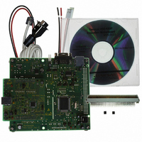
Manufacturer Part Number
M3A-0033
Description
DEV EVALUATION BOARD FOR M66291G
Manufacturer
Renesas Electronics America
Datasheet
1.M3A-0033.pdf
(39 pages)
Specifications of M3A-0033
Main Purpose
USB Controller
Embedded
*
Utilized Ic / Part
M66291
Primary Attributes
*
Secondary Attributes
*
Lead Free Status / RoHS Status
Contains lead / RoHS non-compliant


9.14 DMA Transfer Using *DACK
M66291GP Evaluation Board
Bibliography
M66291GP data sheet
M16C/80 series software manual
In DMA transfer, using memory expansion mode 3, two Dacks of M66291GP can be assign to *CS2 pin and *CS3
pin of M16C/80. The memory map is shown in Figure9-1.
Please set up as shown in Table 9-4 after jumper setup described section “6.2”.
Table 9-4 Jumper Setup of *DACK
Note: JP16 does not function in the memory expansion mode 1. Please refer to the Figure 8-2 for details.
Moreover, in case of connecting M3A-0029B, please refer section “6.2”.
JP
JP17
JP16
(Note)
FFFFFFH
D00000H
C00000H
E00000H
F00000H
000000H
000400H
008000H
100000H
200000H
300000H
400000H
Setting
Short-circuited.
Short-circuited.
Internal reserved area
Internal reserved area
Internal RAM area
*CS3 (1M bytes)
*CS0 (1M bytes)
/CS1 (1M bytes)
/CS2 (1M bytes)
Flash memory
(User area)
Unusable
Unusable
Unusable
SFR area
Figure 9-1 Memory Map 2
Explanation
*DACK0 pin of M66291GP is assigned to *CS2 pin of M
16C/80.
*DACK1 pin of M66291GP is assigned to *CS3 pin of M
16C/80.
- 30 -
FE0000H
Monitor RAM area(1KB)
Monitor program (16K)
(008000H to 008072H)
(008000H to 008076H)
User program area
Vector area( fixed)
User RAM area
Area for 66290
Area for 66291
Dack0 settable
Unusable area
Unusable area
Dack1 settable
Unusable
USB enable register
Monitor program
Unusable area
Special page
Vector table
M3A-0033
Unusable
Unusable
Unusabl
Unusabl
Unusabl
Unusabl
Unusabl
Unusabl
Reset
FFBE00H
FFC000H
FFFE00H
FFFFDCH
FFFFFFH
Related parts for M3A-0033
Image
Part Number
Description
Manufacturer
Datasheet
Request
R

Part Number:
Description:
DEV EVALUATION BOARD FOR M66592
Manufacturer:
Renesas Electronics America
Part Number:
Description:
DEV EVALUATION KIT FOR M66596
Manufacturer:
Renesas Electronics America
Datasheet:
Part Number:
Description:
DEV EVALUATION BOARD FOR M66591G
Manufacturer:
Renesas Electronics America
Part Number:
Description:
M35054/M35055-XXXSP/FP EVAL BOAR
Manufacturer:
Renesas Electronics America
Part Number:
Description:
DEV M35070/71-XXXFP,M35047-XXXFP
Manufacturer:
Renesas Electronics America
Part Number:
Description:
DEV EVALUATION BOARD 38K0/38K2 G
Manufacturer:
Renesas Electronics America

Part Number:
Description:
KIT STARTER FOR M16C/29
Manufacturer:
Renesas Electronics America
Datasheet:

Part Number:
Description:
KIT STARTER FOR R8C/2D
Manufacturer:
Renesas Electronics America
Datasheet:

Part Number:
Description:
R0K33062P STARTER KIT
Manufacturer:
Renesas Electronics America
Datasheet:

Part Number:
Description:
KIT STARTER FOR R8C/23 E8A
Manufacturer:
Renesas Electronics America
Datasheet:

Part Number:
Description:
KIT STARTER FOR R8C/25
Manufacturer:
Renesas Electronics America
Datasheet:
Part Number:
Description:
KIT STARTER H8S2456 SHARPE DSPLY
Manufacturer:
Renesas Electronics America
Datasheet:

Part Number:
Description:
KIT STARTER FOR R8C38C
Manufacturer:
Renesas Electronics America
Datasheet:

Part Number:
Description:
KIT STARTER FOR R8C35C
Manufacturer:
Renesas Electronics America
Datasheet:

Part Number:
Description:
KIT STARTER FOR R8CL3AC+LCD APPS
Manufacturer:
Renesas Electronics America
Datasheet: