CDB5581 Cirrus Logic Inc, CDB5581 Datasheet - Page 6
CDB5581
Manufacturer Part Number
CDB5581
Description
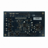
BOARD EVAL FOR CS5581 ADC
Manufacturer
Cirrus Logic Inc
Type
A/Dr
Datasheet
1.CDB5581.pdf
(26 pages)
Specifications of CDB5581
Number Of Adc's
1
Number Of Bits
16
Sampling Rate (per Second)
200k
Data Interface
Serial
Inputs Per Adc
2 Single
Input Range
±2.048 V
Power (typ) @ Conditions
85mW @ 200kSPS
Voltage Supply Source
Dual ±
Operating Temperature
-40°C ~ 85°C
Utilized Ic / Part
CS5581
Product
Data Conversion Development Tools
Conversion Rate
200 KSPS
Resolution
16 bit
Maximum Clock Frequency
16 MHz
Interface Type
SPI
Supply Voltage (max)
3.3 V
Supply Voltage (min)
- 2.5 V
For Use With/related Products
CS5581
Lead Free Status / RoHS Status
Contains lead / RoHS non-compliant
Lead Free Status / RoHS Status
Lead free / RoHS Compliant, Contains lead / RoHS non-compliant
Other names
598-1559


3. HARDWARE DESCRIPTION
3.1
Observe the following limits to ensure the CDB5581 component ratings are not exceeded.
3.2
Power supply connections and requirements are specified in Table 1. below.
Important: It is recommended that all power supplies be isolated from utility ground to prevent the intro-
duction of a ground loop. One ground connection may already exist through the serial port connection to
utility ground. Using the Cirrus Logic CapturePlus II system simplifies making connections to the
CDB5581 by providing electrical isolation between the two.
Using twisted/shielded wire will reduce electrical noise induced onto the power supply cables.
Power supplies are to be adequately regulated and sufficiently low noise to meet the application require-
ments.
3.3
3.3.1
The analog input signal connections to the input buffers are made at the IN_A and IN_B connectors, as
specified in Table 2.
There are two analog input channels on the evaluation board. Each analog input channel consists of a
low-noise amplifier configured as a unity gain non-inverting buffer. The buffers utilize a Cirrus Logic
CS3004 precision, low-noise, low-voltage, dual opamp.. These op-amps enable both the inputs and out-
puts of the analog input buffer to operate virtually rail to rail. The channel input impedance is 50 Ohms.
6
+2.5 V DC, ±5%, <50 mA
+3.3 V DC, ±5%, <50 mA
-2.5 V DC, ±5%, <50 mA
Power Supply
Absolute Maximum Ratings
• CS5581
• CS3004
Power Supply
Requirement
Analog Section
Analog Input Buffers
Channel
IN_A
IN_B
– The absolute maximum supply voltage that can be applied to the +3.3V power supply
– The absolute maximum power supply voltage that can be applied between pins VL and V1-
– The absolute maximum power supply voltage that can be applied between the +2.5V and
connection is +3.6V.
is 6.1 V.
-2.5V power supply connections is +5.5V.
Power Supply
Analog Input
Connection
Connection
Table 1. Power Supply Connections
Table 2. Analog Input Connections
E16
J10
J11
E5
E9
-2.048 V to +2.048 V
-2.048 V to +2.048 V
Ground Return
Voltage Range
Input Signal
Associated
E13
E3
E7
TP2, TP1 (GND)
TP4, TP3 (GND)
TP6, TP5 (GND)
Associated
Test Points
Impedance
50 Ohms
50 Ohms
CDB5581
DS796DB3
Related parts for CDB5581
Image
Part Number
Description
Manufacturer
Datasheet
Request
R

Part Number:
Description:
Development Kit
Manufacturer:
Cirrus Logic Inc
Datasheet:
Part Number:
Description:
Development Kit
Manufacturer:
Cirrus Logic Inc
Datasheet:


Part Number:
Description:
High-efficiency PFC + Fluorescent Lamp Driver Reference Design
Manufacturer:
Cirrus Logic Inc
Datasheet:
Part Number:
Description:
Development Kit
Manufacturer:
Cirrus Logic Inc
Datasheet:
Part Number:
Description:
Development Kit
Manufacturer:
Cirrus Logic Inc
Datasheet:

Part Number:
Description:
Development Kit
Manufacturer:
Cirrus Logic Inc
Datasheet:
Part Number:
Description:
Development Kit
Manufacturer:
Cirrus Logic Inc
Datasheet:
Part Number:
Description:
Development Kit
Manufacturer:
Cirrus Logic Inc
Datasheet:
Part Number:
Description:
Development Kit
Manufacturer:
Cirrus Logic Inc
Datasheet:

Part Number:
Description:
EVALUATION BOARD FOR CS8427
Manufacturer:
Cirrus Logic Inc
Datasheet:

Part Number:
Description:
BOARD EVAL FOR CS8416 RCVR
Manufacturer:
Cirrus Logic Inc
Datasheet:

Part Number:
Description:
EVALUATION BOARD FOR CS8420
Manufacturer:
Cirrus Logic Inc
Datasheet:

Part Number:
Description:
KIT DEVELOPMENT EP9315 ARM9
Manufacturer:
Cirrus Logic Inc
Datasheet:

Part Number:
Description:
KIT DEVELOPMENT EP9302 ARM9
Manufacturer:
Cirrus Logic Inc
Datasheet: