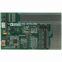
EVAL-AD7794EBZ Analog Devices Inc, EVAL-AD7794EBZ Datasheet
EVAL-AD7794EBZ
Specifications of EVAL-AD7794EBZ


Related parts for EVAL-AD7794EBZ


EVAL-AD7794EBZ Summary of contents
Page 1
FEATURES effective bits RMS noise 4.17 Hz 16.7 Hz Current: 400 μA typical Power-down: 1 μA maximum Low noise, programmable gain, instrumentation amp Band gap reference with 4 ppm/°C drift typical ...
Page 2
AD7794/AD7795 TABLE OF CONTENTS Features .............................................................................................. 1 Applications....................................................................................... 1 General Description ......................................................................... 1 Functional Block Diagram .............................................................. 1 Revision History ............................................................................... 2 Specifications..................................................................................... 3 Timing Characteristics..................................................................... 8 Timing Diagrams.............................................................................. 9 Absolute Maximum Ratings.......................................................... 10 ESD Caution................................................................................ 10 Pin Configuration and ...
Page 3
SPECIFICATIONS 5.25 V, GND = 0 V, all specifications Table 1. Parameter 1 CHOP ENABLED Output Update Rate 2 No Missing Codes AD7794 AD7795 Resolution ...
Page 4
AD7794/AD7795 1 Parameter Common-Mode Rejection AD7794B/AD7795B @ Hz Hz AD7794C @ Hz Hz CHOP DISABLED Output Update Rate ...
Page 5
Parameter 2, 6 Normal Mode Rejection Internal Clock @ 50 Hz External Clock @ 50 Hz Common-Mode Rejection AD7794B/AD7795B @ ...
Page 6
AD7794/AD7795 1 Parameter BIAS VOLTAGE GENERATOR V BIAS V Generator Start-Up Time BIAS TEMPERATURE SENSOR Accuracy Sensitivity LOW-SIDE POWER SWITCH Allowable Current DIGITAL OUTPUTS (P1 and P2 Output High Voltage Output ...
Page 7
Parameter LOGIC OUTPUT (INCLUDING CLK Output High Voltage Output Low Voltage Output High Voltage Output Low Voltage 2 OL Floating-State Leakage Current Floating-State Output Capacitance ...
Page 8
AD7794/AD7795 TIMING CHARACTERISTICS 5.25 V, GND = 0 V, Input Logic Input Logic Table 2. Parameter 1, 2 Limit ...
Page 9
TIMING DIAGRAMS DOUT/RDY ( MSB SCLK ( INPUT OUTPUT Figure 3. Read Cycle Timing Diagram CS ( SCLK ( DIN ...
Page 10
AD7794/AD7795 ABSOLUTE MAXIMUM RATINGS T = 25°C, unless otherwise noted. A Table 3. Parameter AV to GND GND DD Analog Input Voltage to GND Reference Input Voltage to GND Digital Input Voltage to GND Digital Output Voltage ...
Page 11
PIN CONFIGURATION AND FUNCTION DESCRIPTIONS Table 4. Pin Function Descriptions Pin No. Mnemonic Description 1 SCLK Serial Clock Input. This serial clock input is for data transfers to and from the ADC. The SCLK has a Schmitt- triggered input, making ...
Page 12
AD7794/AD7795 Pin No. Mnemonic Description 18 AIN4(−)/REFIN2(−) Analog Input/Negative Reference Input. AIN4(−) is the negative terminal of the differential analog input pair AIN4(+)/AIN4(−). This pin also functions as the negative reference input for REFIN2. This reference input can lie anywhere ...
Page 13
RMS NOISE AND RESOLUTION SPECIFICATIONS The AD7794/AD7795 can be operated with chop enabled or chop disabled, allowing the ADC to be optimized for switching time or drift performance. With chop enabled, the settling time is two times the conversion time. ...
Page 14
AD7794/AD7795 Internal Reference Table 8 shows the AD7794/AD7795 rms noise for some of the update rates and gain settings. The numbers given are for the bipolar input range with the internal 1.17 V reference. These numbers are typical and are ...
Page 15
CHOP DISABLED With chop disabled, the switching time or settling time is reduced by a factor of two. However, periodic offset calibrations may now be required to remove offset and offset drift. When chop is disabled, the AMP-CM bit in ...
Page 16
AD7794/AD7795 TYPICAL PERFORMANCE CHARACTERISTICS 8388800 8388750 8388700 8388650 8388600 8388550 8388500 8388450 0 200 400 600 READING NUMBER Figure 6. Typical Noise Plot for the AD7794 (Internal Reference, Gain = 64, Update Rate = 16.7 Hz, Chop Enabled ...
Page 17
ON-CHIP REGISTERS The ADC is controlled and configured via a number of on-chip registers that are described in the following sections. In the following descriptions, set implies a Logic 1 state and cleared implies a Logic 0 state, unless otherwise ...
Page 18
AD7794/AD7795 STATUS REGISTER RS2, RS1, RS0 = Power-On/Reset = 0x80 (AD7795)/0x88 (AD7794) The status register is an 8-bit read-only register. To access the ADC status register, the user must write to the communications register, select the next ...
Page 19
MODE REGISTER RS2, RS1, RS0 = Power-On/Reset = 0x000A The mode register is a 16-bit read/write register that is used to select the operating mode, the update rate, and the clock source. Table 17 outlines the bit ...
Page 20
AD7794/AD7795 Table 18. Operating Modes MD2 MD1 MD0 Mode Continuous Conversion Mode (Default). In continuous conversion mode, the ADC continuously performs conversions and places the result in the data register. RDY goes low when a conversion is ...
Page 21
Table 19. Update Rates Available (Chop Enabled) FS3 FS2 FS1 FS0 470 242 123 ...
Page 22
AD7794/AD7795 CONFIGURATION REGISTER RS2, RS1, RS0 = Power-On/Reset = 0x0710 The configuration register is a 16-bit read/write register that is used to configure the ADC for unipolar or bipolar mode, enable or disable the buffer, enable or ...
Page 23
Bit No. Mnemonic Description CON5 REF_DET Enables the reference detect function. When set, the NOXREF bit in the status register indicates when the external reference being used by the ADC is open circuit or less than 0.5 V. When cleared, ...
Page 24
AD7794/AD7795 DATA REGISTER RS2, RS1, RS0 = Power-On/Reset = 0x0000(AD7795), 0x000000 (AD7794) The conversion result from the ADC is stored in this data register. This is a read-only register. On completion of a read operation from this ...
Page 25
OFFSET REGISTER RS2, RS1, RS0 = Power-On/Reset = 0x8000 (AD7795), 0x800000 (AD7794)) The offset register is a 16-bit register on the AD7795 and a 24-bit register on the AD7794. The offset register holds the offset calibration coefficient ...
Page 26
AD7794/AD7795 ADC CIRCUIT INFORMATION OVERVIEW The AD7794/AD7795 are low power ADCs that incorporate a ∑-Δ modulator, buffer, reference, in-amp, and on-chip digital filtering, which are intended for the measurement of wide dynamic range, low frequency signals (such as those in ...
Page 27
FREQUENCY (Hz) Figure 13. Filter Response with Update Rate = 4.17 Hz (Chop Enabled) 0 –20 –40 –60 –80 –100 100 120 140 FREQUENCY ...
Page 28
AD7794/AD7795 0 –20 –40 –60 –80 –100 0 500 1000 1500 FREQUENCY (Hz) Figure 19. Filter Response at 242 Hz Update Rate (Chop Disabled) 0 –10 –20 –30 –40 –50 –60 0 1000 2000 3000 4000 5000 6000 7000 8000 ...
Page 29
CS 0x08 DIN DOUT/RDY SCLK CS DIN DOUT/RDY SCLK CS 0x5C DIN DOUT/RDY SCLK 0x200A Figure 21. Single Conversion 0x58 DATA Figure 22. Continuous Conversion DATA Figure 23. Continuous Read Rev Page AD7794/AD7795 0x58 DATA ...
Page 30
AD7794/AD7795 Single Conversion Mode In single conversion mode, the AD7794/AD7795 are placed in shutdown mode between conversions. When a single conversion is initiated by setting MD2 to 0, MD1 to 0, and MD0 the mode register, the ...
Page 31
CIRCUIT DESCRIPTION ANALOG INPUT CHANNEL The AD7794/AD7795 have six differential analog input channels. These are connected to the on-chip buffer amplifier when the devices are operated in buffered mode. When in unbuffered mode, the channels connect directly to the modulator. ...
Page 32
AD7794/AD7795 DATA OUTPUT CODING When the ADC is configured for unipolar operation, the output code is natural (straight) binary with a zero differential input voltage resulting in a code of 00...00, a miscalled voltage resulting in a code of 100...000, ...
Page 33
If the AD7794/AD7795 are used in nonratiometric applications, a low noise reference should ...
Page 34
AD7794/AD7795 one conversion cycle when chop is disabled. For higher gains, four conversion cycles are required to perform the full-scale calibration when chop is enabled, and two conversion cycles when chop is disabled. DOUT/ RDY goes high when the calibration ...
Page 35
APPLICATIONS INFORMATION The AD7794/AD7795 offer low cost, high resolution analog-to- digital functions. Because the analog-to-digital function is provided by a ∑-Δ architecture, it makes the parts more immune to noisy environments, making them ideal for use in sensor measurement, and ...
Page 36
... Thin Shrink Small Outline Package [TSSOP] 24-Lead Thin Shrink Small Outline Package [TSSOP] 24-Lead Thin Shrink Small Outline Package [TSSOP] 24-Lead Thin Shrink Small Outline Package [TSSOP] 24-Lead Thin Shrink Small Outline Package [TSSOP] Evaluation Board Evaluation Board D04854-0-3/07(D) Rev Page 8° 0.75 0° ...