EVAL-AD7794EBZ Analog Devices Inc, EVAL-AD7794EBZ Datasheet - Page 26
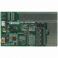
EVAL-AD7794EBZ
Manufacturer Part Number
EVAL-AD7794EBZ
Description
BOARD EVALUATION FOR AD7794
Manufacturer
Analog Devices Inc
Specifications of EVAL-AD7794EBZ
Number Of Adc's
1
Number Of Bits
24
Sampling Rate (per Second)
470
Data Interface
SPI™, QSPI™, MICROWIRE™, and DSP
Inputs Per Adc
6 Differential
Input Range
±VREF/gain
Power (typ) @ Conditions
2.5mW @ 470SPS
Voltage Supply Source
Analog and Digital
Operating Temperature
-40°C ~ 105°C
Utilized Ic / Part
AD7794
Lead Free Status / RoHS Status
Lead free / RoHS Compliant


AD7794/AD7795
ADC CIRCUIT INFORMATION
OVERVIEW
The AD7794/AD7795 are low power ADCs that incorporate a
∑-Δ modulator, buffer, reference, in-amp, and on-chip digital
filtering, which are intended for the measurement of wide
dynamic range, low frequency signals (such as those in pressure
transducers), weigh scales, and temperature measurement
applications.
Each part has six differential inputs that can be buffered or
unbuffered. The devices operate with an internal 1.17 V refer-
ence or by using an external reference. Figure 12 shows the
basic connections required to operate the parts.
The output rate of the AD7794/AD7795 (f
grammable. The allowable update rates, along with the
corresponding settling times, are listed in Table 19 for chop
enabled. With chop disabled, the allowable update rates remain
unchanged, but the settling time equals 1/f
rejection is the major function of the digital filter. Simultaneous
OUT–
IN+
IN–
OUT+
OUT–
IN+
IN–
V
DD
R
CM
OUT+
ADC
ADC
) is user pro-
. Normal mode
REFIN1(+)
AIN1(+)
AIN1(–)
AIN2(+)
AIN2(–)
AIN3(+)
AIN3(–)
REFIN2(+)
REFIN2(–)
IOUT1
REFIN1(–)
PSW
Figure 12. Basic Connection Diagram
GND
Rev. D | Page 26 of 36
MUX
GND
AV
GND
V
DD
DD
BUF
V
50 Hz and 60 Hz rejection is optimized when the update rate
equals 16.7 Hz or less, as notches are placed at both 50 Hz and
60 Hz with these update rates (see Figure 14).
The AD7794/AD7795 use slightly different filter types,
depending on the output update rate, so that the rejection of
quantization noise and device noise is optimized. When the
update rate is 4.17 Hz to 12.5 Hz, a Sinc3 filter along with an
averaging filter is used. When the update rate is 16.7 Hz to
39 Hz, a modified Sinc3 filter is used. This filter gives
simultaneous 50 Hz/60 Hz rejection when the update rate
equals 16.7 Hz. A Sinc4 filter is used when the update rate is
50 Hz to 242 Hz. Finally, an integrate-only filter is used when
the update rate equals 470 Hz. Figure 13 to Figure 16 show the
frequency response of the different filter types for some of the
update rates when chop is enabled. In this mode, the settling
time equals twice the update rate. Figure 17 to Figure 20 show
the filter response with chop disabled.
DD
IN-AMP
CLK
AD7794/AD7795
ADC
INTERNAL
Σ-Δ
CLOCK
INTERFACE
CONTROL
SERIAL
LOGIC
AND
DOUT/RDY
DIN
SCLK
CS
DV
DD
Related parts for EVAL-AD7794EBZ
Image
Part Number
Description
Manufacturer
Datasheet
Request
R


Part Number:
Description:
BOARD EVAL FOR SI270X-A
Manufacturer:
Silicon Laboratories Inc
Datasheet:

Part Number:
Description:
BUCK CONV REF DESIGN KIT IP1201
Manufacturer:
International Rectifier
Datasheet:
Part Number:
Description:
BOARD DEMO SYNC DUAL BUCK CNVTER
Manufacturer:
International Rectifier
Datasheet:
Part Number:
Description:
BOARD DEMO SYNC BUCK CONVETER
Manufacturer:
International Rectifier
Datasheet:

Part Number:
Description:
EVALBOARD/EB Omnidirectional microphone - Analog
Manufacturer:
Analog Devices
Datasheet:
Part Number:
Description:
EVALBOARD/EB Omnidirectional microphone - Analog
Manufacturer:
Analog Devices
Datasheet:


Part Number:
Description:
BOARD EVAL LED DRIVER LT3756
Manufacturer:
Linear Technology
Datasheet:

Part Number:
Description:
BOARD EVAL FOR AD7741/7742
Manufacturer:
Analog Devices Inc
Datasheet:

Part Number:
Description:
±1.7g Dual-Axis IMEMS Accelerometer Evaluation Board
Manufacturer:
Analog Devices Inc
Datasheet:

Part Number:
Description:
IC MULTIPLIER ANALOG 8-SOIC T/R
Manufacturer:
Analog Devices Inc
Datasheet:

Part Number:
Description:
IC ANALOG MULTIPLIER 8-DIP
Manufacturer:
Analog Devices Inc
Datasheet:
Part Number:
Description:
IC ANALOG MULTIPLIER 8-SOIC
Manufacturer:
Analog Devices Inc
Datasheet:
Part Number:
Description:
IC ANALOG MULTIPLIER 8-DIP
Manufacturer:
Analog Devices Inc
Datasheet: