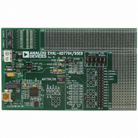
EVAL-AD7794EBZ Analog Devices Inc, EVAL-AD7794EBZ Datasheet - Page 22
EVAL-AD7794EBZ
Manufacturer Part Number
EVAL-AD7794EBZ
Description
BOARD EVALUATION FOR AD7794
Manufacturer
Analog Devices Inc
Specifications of EVAL-AD7794EBZ
Number Of Adc's
1
Number Of Bits
24
Sampling Rate (per Second)
470
Data Interface
SPI™, QSPI™, MICROWIRE™, and DSP
Inputs Per Adc
6 Differential
Input Range
±VREF/gain
Power (typ) @ Conditions
2.5mW @ 470SPS
Voltage Supply Source
Analog and Digital
Operating Temperature
-40°C ~ 105°C
Utilized Ic / Part
AD7794
Lead Free Status / RoHS Status
Lead free / RoHS Compliant


AD7794/AD7795
CONFIGURATION REGISTER
RS2, RS1, RS0 = 0, 1, 0; Power-On/Reset = 0x0710
The configuration register is a 16-bit read/write register that is
used to configure the ADC for unipolar or bipolar mode, enable
or disable the buffer, enable or disable the burnout currents,
select the gain, and select the analog input channel.
CON15
VBIAS1(0)
CON7
REFSEL1(0)
Table 20. Configuration Register Bit Designations
Bit No.
CON15 to
CON14
CON13
CON12
CON11
CON10 to
CON8
CON7 to
CON6
BO
Mnemonic
VBIAS1 to VBIAS0
U/B
BOOST
G2 to G0
REFSEL1/REFSEL0
CON14
VBIAS0(0)
CON6
REFSEL0(0)
Description
Bias Voltage Generator Enable. The negative terminal of the analog inputs can be biased up to AV
These bits are used in conjunction with the BOOST bit.
VBIAS1
0
0
1
1
Burnout Current Enable Bit. This bit must be programmed with a Logic 0 for correct operation. When this
bit is set to 1 by the user, the 100 nA current sources in the signal path are enabled. When BO = 0, the
burnout currents are disabled. The burnout currents can be enabled only when the buffer or in-amp is active.
Unipolar/Bipolar Bit. Set by user to enable unipolar coding, that is, zero differential input results in
0x000000 output and a full-scale differential input results in 0xFFFFFF output. Cleared by the user to
enable bipolar coding. Negative full-scale differential input results in an output code of 0x000000, zero
differential input results in an output code of 0x800000, and positive full-scale differential input results in
an output code of 0xFFFFFF.
This bit is used in conjunction with the VBIAS1 and VBIAS0 bits. When set, the current consumed by the
bias voltage generator is increased, which reduces its power-up time.
Gain Select Bits.
Written by the user to select the ADC input range as follows:
G2
0
0
0
0
1
1
1
1
Reference Select Bits.
The reference source for the ADC is selected using these bits.
REFSEL1
0
0
1
1
CON13
BO(0)
CON5
REF_DET(0)
G1
0
0
1
1
0
0
1
1
REFSEL0
0
1
0
1
G0
0
1
0
1
0
1
0
1
VBIAS0
0
1
0
1
Rev. D | Page 22 of 36
CON12
U/B(0)
CON4
BUF(1)
Reference Source
Internal 1.17 V reference
External reference applied between REFIN1(+) and REFIN1(−)
External reference applied between REFIN2(+) and REFIN2(−)
Reserved
Gain
1 (in-amp not
used)
2 (in-amp not
used)
4
8
16
32
64
128
Table 20 outlines the bit designations for the filter register.
CON0 through CON15 indicate the bit locations. CON denotes
that the bits are in the configuration register. CON15 is the first
bit of the data stream. The number in parentheses indicates the
power-on/reset default status of that bit.
CON11
BOOST(0)
CON3
CH3(0)
ADC Input Range (2.5 V Reference)
2.5 V
1.25 V
625 mV
312.5 mV
156.2 mV
78.125 mV
39.06 mV
19.53 mV
Bias Voltage
Bias voltage generator disabled
Bias voltage generator connected to AIN1(−)
Bias voltage generator connected to AIN2(−)
Bias voltage generator connected to AIN3(−)
CON10
G2(1)
CON2
CH2(0)
CON9
G1(1)
CON1
CH1(0)
CON8
G0(1)
CON0
CH0(0)
DD
/2.
Related parts for EVAL-AD7794EBZ
Image
Part Number
Description
Manufacturer
Datasheet
Request
R


Part Number:
Description:
BOARD EVAL FOR SI270X-A
Manufacturer:
Silicon Laboratories Inc
Datasheet:

Part Number:
Description:
BUCK CONV REF DESIGN KIT IP1201
Manufacturer:
International Rectifier
Datasheet:
Part Number:
Description:
BOARD DEMO SYNC DUAL BUCK CNVTER
Manufacturer:
International Rectifier
Datasheet:
Part Number:
Description:
BOARD DEMO SYNC BUCK CONVETER
Manufacturer:
International Rectifier
Datasheet:

Part Number:
Description:
EVALBOARD/EB Omnidirectional microphone - Analog
Manufacturer:
Analog Devices
Datasheet:
Part Number:
Description:
EVALBOARD/EB Omnidirectional microphone - Analog
Manufacturer:
Analog Devices
Datasheet:


Part Number:
Description:
BOARD EVAL LED DRIVER LT3756
Manufacturer:
Linear Technology
Datasheet:

Part Number:
Description:
BOARD EVAL FOR AD7741/7742
Manufacturer:
Analog Devices Inc
Datasheet:

Part Number:
Description:
±1.7g Dual-Axis IMEMS Accelerometer Evaluation Board
Manufacturer:
Analog Devices Inc
Datasheet:

Part Number:
Description:
IC MULTIPLIER ANALOG 8-SOIC T/R
Manufacturer:
Analog Devices Inc
Datasheet:

Part Number:
Description:
IC ANALOG MULTIPLIER 8-DIP
Manufacturer:
Analog Devices Inc
Datasheet:
Part Number:
Description:
IC ANALOG MULTIPLIER 8-SOIC
Manufacturer:
Analog Devices Inc
Datasheet:
Part Number:
Description:
IC ANALOG MULTIPLIER 8-DIP
Manufacturer:
Analog Devices Inc
Datasheet: