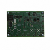
STEVAL-ISA051V1 STMicroelectronics, STEVAL-ISA051V1 Datasheet - Page 24

STEVAL-ISA051V1
Manufacturer Part Number
STEVAL-ISA051V1
Description
BOARD EVAL PM6670S DDR2/3
Manufacturer
STMicroelectronics
Type
DC/DC Switching Converters, Regulators & Controllersr
Specifications of STEVAL-ISA051V1
Design Resources
STEVAL-ISA051V1 Gerber Files STEVAL-ISA051V1 Schematic STEVAL-ISA051V1 Bill of Material
Main Purpose
Special Purpose DC/DC, DDR Memory Supply
Outputs And Type
4, Non-Isolated
Voltage - Output
1.5V, 1.8V
Voltage - Input
4.5 ~ 28V
Regulator Topology
Buck
Board Type
Fully Populated
Utilized Ic / Part
PM6670
Input Voltage
4.5 V to 28 V
Output Voltage
1.8 V, 1.5 V
Product
Power Management Modules
Silicon Manufacturer
ST Micro
Silicon Core Number
PM6670S
Kit Application Type
Power Management
Application Sub Type
DDR2/3 Memory Power Supply Controller
Kit Contents
Board
Lead Free Status / RoHS Status
Lead free / RoHS Compliant
Current - Output
-
Power - Output
-
Frequency - Switching
-
Lead Free Status / Rohs Status
Lead free / RoHS Compliant
For Use With/related Products
PM6670S
Other names
497-8411
Available stocks
Company
Part Number
Manufacturer
Quantity
Price
Company:
Part Number:
STEVAL-ISA051V1
Manufacturer:
STMicroelectronics
Quantity:
1
Device description
7.1.2
24/54
Output ripple compensation and loop stability
The loop is closed connecting the center tap of the output divider (internally, when the fixed
output voltage is chosen, or externally, using the MODE pin in the adjustable output voltage
mode). The feedback node is the negative input of the error comparator, while the positive
input is internally connected to the reference voltage (Vr = 0.9 V). When the feedback
voltage becomes lower than the reference voltage, the PWM comparator goes to high and
sets the control logic, turning on the high-side MOSFET. After the on-time (calculated as
previously described) the system releases the high-side MOSFET and turns on the
synchronous rectifier.
The voltage drop along ground and supply PCB paths, used to connect the output capacitor
to the load, is a source of DC error. Furthermore the system regulates the output voltage
valley, not the average, as shown in
capacitor is an additional source of DC error. To compensate this error, an integrative
network is introduced in the control loop, by connecting the output voltage to the COMP pin
through a capacitor (C
Figure 31. Circuitry for output ripple compensation
The additional capacitor is used to reduce the voltage on the COMP pin when higher than
300 mVpp and is unnecessary for most of applications. The trans conductance amplifier
(gm) generates a current, proportional to the DC error, used to charge the CINT capacitor.
The voltage across the CINT capacitor feeds the negative input of the PWM comparator,
forcing the loop to compensate the total static error. An internal voltage clamp forces the
COMP pin voltage range to ±150 mV with respect to VREF. This is useful to avoid or smooth
output voltage overshoot during a load transient. When the pulse-skip mode is entered, the
clamping range is automatically reduced to 60 mV in order to enhance the recovering
capability. In the ripple amplitude is larger than 150 mV, an additional capacitor CFILT can
be connected between the COMP pin and ground to reduce ripple amplitude, otherwise the
integrator will operate out of its linearity range. This capacitor is unnecessary for most of
applications and can be omitted.
Vr
COMP PIN
VOLTAGE
OUTPUT
VOLTAGE
t
t
INT
ΔV
ΔV
) as shown in
C
Doc ID 14432 Rev 4
C
ESR
ESR
OUT
OUT
C
C
FILT
FILT
Figure 28
C
R
C
R
INT
INT
INT
INT
Figure 31
COMP
VSNS
V
V
. Thus, the voltage ripple on the output
C
C
INT
INT
.
I=g
m
Vr
Vr
(V
1
-Vr)
R
R
Fb2
Fb2
g
g
V
V
m
m
1
1
+
V
V
REF
REF
R
R
Fb1
Fb1
+
-
Comparator
PWM
PM6670S


