STEVAL-ISA051V1 STMicroelectronics, STEVAL-ISA051V1 Datasheet - Page 35
STEVAL-ISA051V1
Manufacturer Part Number
STEVAL-ISA051V1
Description
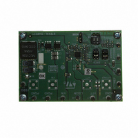
BOARD EVAL PM6670S DDR2/3
Manufacturer
STMicroelectronics
Type
DC/DC Switching Converters, Regulators & Controllersr
Specifications of STEVAL-ISA051V1
Design Resources
STEVAL-ISA051V1 Gerber Files STEVAL-ISA051V1 Schematic STEVAL-ISA051V1 Bill of Material
Main Purpose
Special Purpose DC/DC, DDR Memory Supply
Outputs And Type
4, Non-Isolated
Voltage - Output
1.5V, 1.8V
Voltage - Input
4.5 ~ 28V
Regulator Topology
Buck
Board Type
Fully Populated
Utilized Ic / Part
PM6670
Input Voltage
4.5 V to 28 V
Output Voltage
1.8 V, 1.5 V
Product
Power Management Modules
Silicon Manufacturer
ST Micro
Silicon Core Number
PM6670S
Kit Application Type
Power Management
Application Sub Type
DDR2/3 Memory Power Supply Controller
Kit Contents
Board
Lead Free Status / RoHS Status
Lead free / RoHS Compliant
Current - Output
-
Power - Output
-
Frequency - Switching
-
Lead Free Status / Rohs Status
Lead free / RoHS Compliant
For Use With/related Products
PM6670S
Other names
497-8411
Available stocks
Company
Part Number
Manufacturer
Quantity
Price
Company:

Part Number:
STEVAL-ISA051V1
Manufacturer:
STMicroelectronics
Quantity:
1


PM6670S
7.1.9
7.1.10
Gate drivers
The integrated high-current gate drivers allow using different power MOSFETs. The high-
side driver uses a bootstrap circuit which is supplied by the +5 V rail. The BOOT and
PHASE pins work respectively as supply and return path for the high-side driver, while the
low-side driver is directly fed through VCC and PGND pins.
An important feature of the PM6670S gate drivers is the adaptive anti-cross-conduction
circuitry, which prevents high-side and low-side MOSFETs from being turned on at the same
time. When the high-side MOSFET is turned off, the voltage at the PHASE node begins to
fall. The low-side MOSFET is turned on only when the voltage at the PHASE node reaches
an internal threshold (2.5 V typ.). Similarly, when the low-side MOSFET is turned off, the
high-side one remains off until the LGATE pin voltage is above 1V.
The power dissipation of the drivers is a function of the total gate charge of the external
power MOSFETs and the switching frequency, as shown in the following equation:
Equation 23
The low-side driver has been designed to have a low-resistance pull-down transistor
(0.6 Ω typ.) in order to prevent undesired ignition of the low-side MOSFET due to the Miller
effect.
Reference voltage and bandgap
The 1.237 V internal bandgap reference has a granted accuracy of ±1 % over the
0 °C to 85 °C temperature range. The VREF pin is a buffered replica of the bandgap voltage.
It can supply up to ±100 μA and is suitable to set the intermediate level of MODE, DDRSEL
and DSCG multifunction pins. A 100 nF (min.) bypass capacitor toward SGND is required to
enhance noise rejection. If VREF falls below 0.8 V (typ.), the system detects a fault condition
and all the circuitry is turned OFF.
An internal divider derives a 0.9 V ± 1 % voltage (Vr) from the bandgap. This voltage is used
as a reference by the switching regulator output. The over-voltage protection, the under-
voltage protection and the power good signal are also referred to Vr.
Doc ID 14432 Rev 4
P
D
(
driver
)
=
V
DRV
⋅
Q
g
⋅
f
SW
Device description
35/54
Related parts for STEVAL-ISA051V1
Image
Part Number
Description
Manufacturer
Datasheet
Request
R

Part Number:
Description:
BOARD RGB CTR ST7,STP08C596MTR
Manufacturer:
STMicroelectronics
Datasheet:

Part Number:
Description:
Power Management IC Development Tools Full Speed USB to RS232 Bridge Demo
Manufacturer:
STMicroelectronics
Datasheet:
Part Number:
Description:
Power Management IC Development Tools 2.5W solar eval BRD USB SPV1040 LD39050
Manufacturer:
STMicroelectronics
Datasheet:

Part Number:
Description:
BOARD EVAL FOR MEMS SENSORS
Manufacturer:
STMicroelectronics
Datasheet:

Part Number:
Description:
KIT DEV STARTER ST10F276Z5
Manufacturer:
STMicroelectronics
Datasheet:

Part Number:
Description:
BOARD EVAL HDMI $ VIDEO SWITCH
Manufacturer:
STMicroelectronics
Datasheet:

Part Number:
Description:
BOARD DEMO ACCELEROMETER DIL24
Manufacturer:
STMicroelectronics
Datasheet:

Part Number:
Description:
BOARD STLM75/STDS75/ST72F651
Manufacturer:
STMicroelectronics
Datasheet:

Part Number:
Description:
EVAL BOARD 3AXIS MEMS ACCELLRMTR
Manufacturer:
STMicroelectronics
Datasheet:

Part Number:
Description:
BOARD EVAL 8BIT MICRO + TDE1708
Manufacturer:
STMicroelectronics
Datasheet:
Part Number:
Description:
STMicroelectronics [RIPPLE-CARRY BINARY COUNTER/DIVIDERS]
Manufacturer:
STMicroelectronics
Datasheet:
Part Number:
Description:
STMicroelectronics [LIQUID-CRYSTAL DISPLAY DRIVERS]
Manufacturer:
STMicroelectronics
Datasheet:
Part Number:
Description:
BOARD EVAL FOR MEMS SENSORS
Manufacturer:
STMicroelectronics
Datasheet: