STEVAL-ISA051V1 STMicroelectronics, STEVAL-ISA051V1 Datasheet - Page 6
STEVAL-ISA051V1
Manufacturer Part Number
STEVAL-ISA051V1
Description
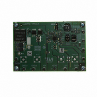
BOARD EVAL PM6670S DDR2/3
Manufacturer
STMicroelectronics
Type
DC/DC Switching Converters, Regulators & Controllersr
Specifications of STEVAL-ISA051V1
Design Resources
STEVAL-ISA051V1 Gerber Files STEVAL-ISA051V1 Schematic STEVAL-ISA051V1 Bill of Material
Main Purpose
Special Purpose DC/DC, DDR Memory Supply
Outputs And Type
4, Non-Isolated
Voltage - Output
1.5V, 1.8V
Voltage - Input
4.5 ~ 28V
Regulator Topology
Buck
Board Type
Fully Populated
Utilized Ic / Part
PM6670
Input Voltage
4.5 V to 28 V
Output Voltage
1.8 V, 1.5 V
Product
Power Management Modules
Silicon Manufacturer
ST Micro
Silicon Core Number
PM6670S
Kit Application Type
Power Management
Application Sub Type
DDR2/3 Memory Power Supply Controller
Kit Contents
Board
Lead Free Status / RoHS Status
Lead free / RoHS Compliant
Current - Output
-
Power - Output
-
Frequency - Switching
-
Lead Free Status / Rohs Status
Lead free / RoHS Compliant
For Use With/related Products
PM6670S
Other names
497-8411
Available stocks
Company
Part Number
Manufacturer
Quantity
Price
Company:

Part Number:
STEVAL-ISA051V1
Manufacturer:
STMicroelectronics
Quantity:
1


Pin settings
2.2
6/54
Pin description
Table 2.
N°
10
11
12
13
14
15
16
17
1
2
3
4
5
6
7
8
9
VTTGND
DDRSEL
VTTSNS
VTTREF
LGATE
MODE
COMP
SGND
DSCG
PGND
VOSC
AVCC
VREF
VSNS
Pin
Pin functions
PG
S5
S3
LDO power ground. Connect to negative terminal of VTT output capacitor.
LDO remote sensing. Connect as close as possible to the load via a low
noise PCB trace.
DDR voltage selector (if MODE is tied to VCC) or pulse-skip/no-audible
pulse-skip selector in adjustable mode (MODE voltage lower than 3 V). See
Section 7.1.4: Mode-of-operation selection on page
Low noise buffered DDR reference voltage. A 22 nF (minimum) ceramic
bypass capacitor is required in order to achieve stability.
Ground reference for analog circuitry, control logic and VTTREF buffer.
Connect together with the thermal pad and VTTGND to a low impedance
ground plane. See the Application Note for details.
+5 V supply for internal logic. Connect to +5 V rail through a simple RC
filtering network.
High accuracy output voltage reference (1.237 V) for multilevel pins setting.
It can deliver up to 50 μA. Connect a 100 nF capacitor between VREF and
SGND in order to enhance noise rejection.
Frequency selection. Connect to the central tap of a resistor divider to set
the desired switching frequency. The pin cannot be left floating. See
Section 7: Device description on page 20
VDDQ output remote sensing. Discharge path for VDDQ in Non-Tracking
Discharge. Input for internal resistor divider that provides VDDQ/2 to
VTTREF and VTT. Connect as close as possible to the load via a low noise
PCB trace.
Mode of operation selector. If MODE pin voltage is higher than 4 V, the fixed
output mode is selected. If MODE pin voltage is lower than 4 V, it is used as
negative input of the error amplifier. See
selection on page
DC voltage error compensation Input for the switching section. Refer
Section 7.1.4: Mode-of-operation selection on page
Discharge mode selection. Refer to
on page 34
Switching controller enable. Connect to S5 system status signal to meet S0-
S5 power management states compliance. See
power management pins on page
Linear regulator enable. Connect to S3 system status signal to meet S0-S5
power management states compliance. See
management pins on page
Power Good signal (open drain output). High when VDDQ output voltage is
within ±10 % of nominal value.
Power ground for the switching section.
Low-side gate driver output.
Doc ID 14432 Rev 4
for tracking/non-tracking discharge or no-discharge options.
30.
38, S3 pin can't be left floating.
Function
38, S5 pin can't be left floating.
Section 7.1.8: VDDQ output discharge
Section 7.1.4: Mode-of-operation
Section 7.3: S3 and S5 power
Section 7.3: S3 and S5
30.
30.
PM6670S
Related parts for STEVAL-ISA051V1
Image
Part Number
Description
Manufacturer
Datasheet
Request
R

Part Number:
Description:
BOARD RGB CTR ST7,STP08C596MTR
Manufacturer:
STMicroelectronics
Datasheet:

Part Number:
Description:
Power Management IC Development Tools Full Speed USB to RS232 Bridge Demo
Manufacturer:
STMicroelectronics
Datasheet:
Part Number:
Description:
Power Management IC Development Tools 2.5W solar eval BRD USB SPV1040 LD39050
Manufacturer:
STMicroelectronics
Datasheet:

Part Number:
Description:
BOARD EVAL FOR MEMS SENSORS
Manufacturer:
STMicroelectronics
Datasheet:

Part Number:
Description:
KIT DEV STARTER ST10F276Z5
Manufacturer:
STMicroelectronics
Datasheet:

Part Number:
Description:
BOARD EVAL HDMI $ VIDEO SWITCH
Manufacturer:
STMicroelectronics
Datasheet:

Part Number:
Description:
BOARD DEMO ACCELEROMETER DIL24
Manufacturer:
STMicroelectronics
Datasheet:

Part Number:
Description:
BOARD STLM75/STDS75/ST72F651
Manufacturer:
STMicroelectronics
Datasheet:

Part Number:
Description:
EVAL BOARD 3AXIS MEMS ACCELLRMTR
Manufacturer:
STMicroelectronics
Datasheet:

Part Number:
Description:
BOARD EVAL 8BIT MICRO + TDE1708
Manufacturer:
STMicroelectronics
Datasheet:
Part Number:
Description:
STMicroelectronics [RIPPLE-CARRY BINARY COUNTER/DIVIDERS]
Manufacturer:
STMicroelectronics
Datasheet:
Part Number:
Description:
STMicroelectronics [LIQUID-CRYSTAL DISPLAY DRIVERS]
Manufacturer:
STMicroelectronics
Datasheet:
Part Number:
Description:
BOARD EVAL FOR MEMS SENSORS
Manufacturer:
STMicroelectronics
Datasheet: