NCP5425SOEVB ON Semiconductor, NCP5425SOEVB Datasheet - Page 14
NCP5425SOEVB
Manufacturer Part Number
NCP5425SOEVB
Description
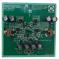
EVAL BOARD FOR NCP5425SO
Manufacturer
ON Semiconductor
Specifications of NCP5425SOEVB
Design Resources
NCP5425SOEVB BOM NCP5425SOEVB Gerber Files NCP5425SOEVB Schematic
Main Purpose
DC/DC, Step Down
Outputs And Type
1, Non-Isolated
Voltage - Output
0.8V
Current - Output
30A
Voltage - Input
4.6 ~ 12 V
Regulator Topology
Buck
Frequency - Switching
300kHz
Board Type
Fully Populated
Utilized Ic / Part
NCP5425
Lead Free Status / RoHS Status
Lead free / RoHS Compliant
Power - Output
-
Lead Free Status / Rohs Status
Lead free / RoHS Compliant
For Use With/related Products
NCP5425SO
Other names
NCP5425SOEVBOS


Output Inductor Selection
inductance, current capability, and DC resistance.
Increasing the inductor value will decrease output voltage
ripple, but degrade transient response. There are many
factors to consider in selecting inductors including cost,
efficiency, EMI and ease of manufacture. The inductor must
be able to handle the peak current at the switching frequency
without saturating, and the copper resistance in the winding
should be kept as low as possible to minimize resistive
power loss.
cores that could be used, such as ferrites, molypermalloy
cores (MPP), and amorphous and powdered iron cores.
Powdered iron cores are particularly suitable due to high
saturation flux density and low loss at high frequencies, a
distributed gap, and they produce very low EMI. The
minimum value of inductance to prevent inductor
saturation, or exceeding the rated FET current, can be
calculated as follows:
where:
where:
number of output capacitors will provide an acceptable
output voltage ripple (1.0% of output voltage is common).
The formula below is used;
where:
The inductor should be selected based on the criteria of
There are a variety of materials and types of magnetic
The inductor ripple current can then be determined by:
After inductor selection, the designer can verify if the
Rearranging, we have:
L
V
V
f
I
D
V
L = inductor value;
D = duty cycle;
f
ESR
DV
DI
V
SW
SW
SW
MIN
IN
OUT
IL
OUT
OUT
L
OUT
(MIN) = minimum design input voltage;
(MAX) = maximum design switch current.
= inductor ripple current;
= switching frequency;
= switching frequency.
= inductor ripple current;
MAX
= minimum inductance value;
= output voltage;
= output voltage;
= output voltage.
L MIN +
= 1.0% ⋅ VOUT = maximum allowable output
= maximum allowable ESR;
voltage ripple (budgeted by the designer);
DI L +
f SW
ESR MAX +
(V IN(MIN) * V OUT )V OUT
DI L +
V OUT
V IN(MIN)
ESR MAX
L
DV OUT
DV OUT
f SW
(1 * D)
DI L
I SW(MAX)
http://onsemi.com
NCP5425
14
where:
yields reasonable inductor peak and valley currents (the
inductor current is a triangular waveform):
where:
Output Capacitor Selection
to yield optimal results. Capacitors should be chosen to
provide acceptable ripple on the regulator output voltage.
Key specifications for output capacitors are ESR
(Equivalent Series Resistance) and ESL (Equivalent Series
Inductance). For best transient response, a combination of
low value/high frequency and bulk capacitors placed close
to the load will be required. To determine the number of
output capacitors the maximum voltage transient allowed
during load transitions has to be specified. The output
capacitors must hold the output voltage within these limits
since the inductor current can not change at the required slew
rate. The output capacitors must therefore have a very low
ESL and ESR.
given by:
where:
change in output voltage due to ESR, ESL, and output
capacitor discharging or charging. Empirical data indicates
that most of the output voltage change (droop or spike,
depending on the load current transition) results from the
total output capacitor ESR.
I L(PEAK) + I OUT )
The number of output capacitors is determined by:
The designer must also verify that the inductor value
These components must be selected and placed carefully
The voltage change during the load current transient is
The designer must independently assign values for the
ESR
I
I
I
DI
DI
DI
Dt = load transient duration time;
ESL = Maximum allowable ESL including capacitors,
ESR = Maximum allowable ESR including capacitors
t
C
TR
L(PEAK)
L(VALLEY)
OUT
OUT
L
OUT
OUT
DV OUT + DI OUT
= output voltage transient response time;
= inductor ripple current.
CAP
= load current;
= output capacitance.
/DD = load current slew rate;
= load transient;
circuit traces, and vias;
and circuit traces;
= maximum ESR per capacitor
= inductor peak current;
Number of capacitors +
= inductor valley current;
(specified in manufacturer’s data sheet).
DI L
2
ESL
Dt
I L(VALLEY) + I OUT )
) ESR )
ESR CAP
ESR MAX
C OUT
t TR
DI L
2
Related parts for NCP5425SOEVB
Image
Part Number
Description
Manufacturer
Datasheet
Request
R

Part Number:
Description:
Dual Synchronous Buck Controller
Manufacturer:
ON Semiconductor
Datasheet:
Part Number:
Description:
ON Semiconductor [VOLTAGE REGULATOR]
Manufacturer:
ON Semiconductor
Datasheet:
Part Number:
Description:
357-036-542-201 CARDEDGE 36POS DL .156 BLK LOPRO
Manufacturer:
ON Semiconductor
Datasheet:
Part Number:
Description:
357-036-542-201 CARDEDGE 36POS DL .156 BLK LOPRO
Manufacturer:
ON Semiconductor
Datasheet:
Part Number:
Description:
357-036-542-201 CARDEDGE 36POS DL .156 BLK LOPRO
Manufacturer:
ON Semiconductor
Datasheet:
Part Number:
Description:
357-036-542-201 CARDEDGE 36POS DL .156 BLK LOPRO
Manufacturer:
ON Semiconductor
Datasheet:
Part Number:
Description:
357-036-542-201 CARDEDGE 36POS DL .156 BLK LOPRO
Manufacturer:
ON Semiconductor
Datasheet:
Part Number:
Description:
357-036-542-201 CARDEDGE 36POS DL .156 BLK LOPRO
Manufacturer:
ON Semiconductor
Datasheet:
Part Number:
Description:
357-036-542-201 CARDEDGE 36POS DL .156 BLK LOPRO
Manufacturer:
ON Semiconductor
Datasheet:
Part Number:
Description:
357-036-542-201 CARDEDGE 36POS DL .156 BLK LOPRO
Manufacturer:
ON Semiconductor
Datasheet:
Part Number:
Description:
357-036-542-201 CARDEDGE 36POS DL .156 BLK LOPRO
Manufacturer:
ON Semiconductor
Datasheet:
Part Number:
Description:
357-036-542-201 CARDEDGE 36POS DL .156 BLK LOPRO
Manufacturer:
ON Semiconductor
Datasheet:
Part Number:
Description:
Manufacturer:
ON Semiconductor
Datasheet:
Part Number:
Description:
Manufacturer:
ON Semiconductor
Datasheet: