NCP5425SOEVB ON Semiconductor, NCP5425SOEVB Datasheet - Page 20
NCP5425SOEVB
Manufacturer Part Number
NCP5425SOEVB
Description
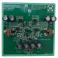
EVAL BOARD FOR NCP5425SO
Manufacturer
ON Semiconductor
Specifications of NCP5425SOEVB
Design Resources
NCP5425SOEVB BOM NCP5425SOEVB Gerber Files NCP5425SOEVB Schematic
Main Purpose
DC/DC, Step Down
Outputs And Type
1, Non-Isolated
Voltage - Output
0.8V
Current - Output
30A
Voltage - Input
4.6 ~ 12 V
Regulator Topology
Buck
Frequency - Switching
300kHz
Board Type
Fully Populated
Utilized Ic / Part
NCP5425
Lead Free Status / RoHS Status
Lead free / RoHS Compliant
Power - Output
-
Lead Free Status / Rohs Status
Lead free / RoHS Compliant
For Use With/related Products
NCP5425SO
Other names
NCP5425SOEVBOS


the Comp 2 voltage excursions during overcurrent faults.
Without this clamp, the output voltage (Vout1 and Vout2)
can overshoot the regulated output voltages when the fault
is removed. For a single output two−phase application the
Mode pin must be floating, which disables the clamp and
permits a larger current−sharing reference voltage range.
The Comp1 pin is always clamped, because it is regulated to
a fixed internal voltage (0.8 V).
Adding External Slope Compensation
stringent load transient requirements. One of the key factors
in achieving tight dynamic voltage regulation is low ESR.
Low ESR at the regulator output results in low output
voltage ripple. The consequence is, however, that very little
voltage ramp exists at the control IC feedback pin (VFB),
resulting in increased regulator sensitivity to noise and the
potential for loop instability. In applications where the
internal slope compensation is insufficient, the performance
of the NCP5425−based regulator can be improved through
the addition of a fixed amount of external slope
compensation at the output of the PWM Error Amplifier (the
COMP pin) during the regulator off−time. Referring to
Figure 8, the amount of voltage ramp at the COMP pin is
dependent on the gate voltage of the lower (synchronous)
FET and the value of resistor divider formed by R1and R2.
where:
V SLOPECOMP + V GATE(L)
Grounding the Mode pin enables an internal clamp to limit
Today’s voltage regulators are expected to meet very
V
V
R1, R2 = voltage divider resistors;
t = t
SLOPECOMP
GATE(L)
ON
or t
= lower MOSFET gate voltage;
OFF
Q1
Q2
Error Amp
= amount of slope added;
Master
(switch off−time);
−
+
Vfb1
Vref1
0.8 V Ref.
Internal
L1
R1 ) R2
R2
Figure 15. Dual Output Configuration
C1
Vout1
(1−e −1 t )
http://onsemi.com
R1
R2
NCP5425
Vin
20
using the Controller 1 feedback voltage. This will provide a
0.8 V reference for regulation, and also causes the
Controller 2 output to track the Controller 1 output during
transients. With a voltage reference established and the
Mode pin floating, Controller 2 can function as an
independent Buck regulator.
compensation scheme results in improved control loop
stability provided that the RC filter time constant is smaller
than the off−time cycle duration (time during which the lower
MOSFET is conducting). It is important that the series
combination of R1 and R2 is high enough in resistance to
avoid loading the GATE(L) pin. Also, C1 should be very
small (less than a few nF) to avoid heating the part.
R3
R4
The simplest way to provide a Controller 2 reference is by
The artificial voltage ramp created by the slope
t = RC constant determined by C1 and the parallel
Figure 16. RC Filter Provides the Proper Voltage
Ramp at the Beginning of each On−Time Cycle
combination of R1, R2 neglecting the low driver
output impedance.
Vout2
NCP5425
GATE(L)
C2
COMP
L2
Vfb2
Vref2
+
−
R2
Error Amp
Slave
C1
To Synchronous
Q3
Q4
R1
FET
Related parts for NCP5425SOEVB
Image
Part Number
Description
Manufacturer
Datasheet
Request
R

Part Number:
Description:
Dual Synchronous Buck Controller
Manufacturer:
ON Semiconductor
Datasheet:
Part Number:
Description:
ON Semiconductor [VOLTAGE REGULATOR]
Manufacturer:
ON Semiconductor
Datasheet:
Part Number:
Description:
357-036-542-201 CARDEDGE 36POS DL .156 BLK LOPRO
Manufacturer:
ON Semiconductor
Datasheet:
Part Number:
Description:
357-036-542-201 CARDEDGE 36POS DL .156 BLK LOPRO
Manufacturer:
ON Semiconductor
Datasheet:
Part Number:
Description:
357-036-542-201 CARDEDGE 36POS DL .156 BLK LOPRO
Manufacturer:
ON Semiconductor
Datasheet:
Part Number:
Description:
357-036-542-201 CARDEDGE 36POS DL .156 BLK LOPRO
Manufacturer:
ON Semiconductor
Datasheet:
Part Number:
Description:
357-036-542-201 CARDEDGE 36POS DL .156 BLK LOPRO
Manufacturer:
ON Semiconductor
Datasheet:
Part Number:
Description:
357-036-542-201 CARDEDGE 36POS DL .156 BLK LOPRO
Manufacturer:
ON Semiconductor
Datasheet:
Part Number:
Description:
357-036-542-201 CARDEDGE 36POS DL .156 BLK LOPRO
Manufacturer:
ON Semiconductor
Datasheet:
Part Number:
Description:
357-036-542-201 CARDEDGE 36POS DL .156 BLK LOPRO
Manufacturer:
ON Semiconductor
Datasheet:
Part Number:
Description:
357-036-542-201 CARDEDGE 36POS DL .156 BLK LOPRO
Manufacturer:
ON Semiconductor
Datasheet:
Part Number:
Description:
357-036-542-201 CARDEDGE 36POS DL .156 BLK LOPRO
Manufacturer:
ON Semiconductor
Datasheet:
Part Number:
Description:
Manufacturer:
ON Semiconductor
Datasheet:
Part Number:
Description:
Manufacturer:
ON Semiconductor
Datasheet: