NCP5425SOEVB ON Semiconductor, NCP5425SOEVB Datasheet - Page 3
NCP5425SOEVB
Manufacturer Part Number
NCP5425SOEVB
Description
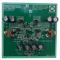
EVAL BOARD FOR NCP5425SO
Manufacturer
ON Semiconductor
Specifications of NCP5425SOEVB
Design Resources
NCP5425SOEVB BOM NCP5425SOEVB Gerber Files NCP5425SOEVB Schematic
Main Purpose
DC/DC, Step Down
Outputs And Type
1, Non-Isolated
Voltage - Output
0.8V
Current - Output
30A
Voltage - Input
4.6 ~ 12 V
Regulator Topology
Buck
Frequency - Switching
300kHz
Board Type
Fully Populated
Utilized Ic / Part
NCP5425
Lead Free Status / RoHS Status
Lead free / RoHS Compliant
Power - Output
-
Lead Free Status / Rohs Status
Lead free / RoHS Compliant
For Use With/related Products
NCP5425SO
Other names
NCP5425SOEVBOS


Stresses exceeding Maximum Ratings may damage the device. Maximum Ratings are stress ratings only. Functional operation above the
Recommended Operating Conditions is not implied. Extended exposure to stresses above the Recommended Operating Conditions may affect
device reliability.
1. 60 to 150 seconds maximum above 183°C, 260°C peak.
MAXIMUM RATINGS
MAXIMUM RATINGS
Operating Junction Temperature, T
Storage Temperature Range, T
ESD Susceptibility (Human Body Model)
ESD Susceptibility (Machine Model)
Thermal Resistance, Junction−to−Air
Moisture Sensitivity Level (MSL)
Lead Temperature Soldering: Reflow: (Note 1)
GATE(H)1
GATE(L)1
V
COMP1, COMP2
FB1
Pin Symbol
IS+1, IS+2
IS−1, IS−2
, V
MODE
R
GND
BST
V
FB2
OSC
CC
,
,
GATE(H)2
GATE(L)2
, V
REF2
J
J
Dual or Single Output Select
Compensation Capacitor for
Negative Current Sense for
Voltage Feedback Input for
Positive Current Sense for
Power Input for GATE(H)1
Low−Side FET Driver for
High−Side FET Driver
Oscillator Resistor
for Channel 1 or 2
IC Power Input
Channel 1 or 2
Channel 1 or 2
Channel 1 or 2
Channel 1 or 2
Channel 1 or 2
Pin Name
Ground
Rating
GATE(H)2
http://onsemi.com
NCP5425
3
100 mV
V
4.0 V
6.0 V
5.0 V
6.0 V
6.0 V
3.5 V
16 V
20 V
16 V
23 V
MAX
−0.3 V
−0.3 V
−0.3 V
−0.3 V
−0.3 V
−0.3 V
−0.3 V
−0.3 V
−0.3 V
−0.3 V
V
0 V
MIN
200 mA DC
200 mA DC
200 mA DC
2.0 A Peak
2.0 A Peak
2.0 A Peak
−65 to 150
260 peak
I
SOURCE
1.0 mA
1.0 mA
1.0 mA
1.0 mA
1.0 mA
Value
150
200
140
N/A
N/A
N/A
2.0
1
200 mA DC
200 mA DC
200 mA DC
200 mA DC
2.0 A Peak
2.0 A Peak
2.0 A Peak
2.0 A Peak
1.0 mA
1.0 mA
1.0 mA
1.0 mA
1.0 mA
°C/W
I
Unit
SINK
N/A
N/A
kV
°C
°C
°C
V
Related parts for NCP5425SOEVB
Image
Part Number
Description
Manufacturer
Datasheet
Request
R

Part Number:
Description:
Dual Synchronous Buck Controller
Manufacturer:
ON Semiconductor
Datasheet:
Part Number:
Description:
ON Semiconductor [VOLTAGE REGULATOR]
Manufacturer:
ON Semiconductor
Datasheet:
Part Number:
Description:
357-036-542-201 CARDEDGE 36POS DL .156 BLK LOPRO
Manufacturer:
ON Semiconductor
Datasheet:
Part Number:
Description:
357-036-542-201 CARDEDGE 36POS DL .156 BLK LOPRO
Manufacturer:
ON Semiconductor
Datasheet:
Part Number:
Description:
357-036-542-201 CARDEDGE 36POS DL .156 BLK LOPRO
Manufacturer:
ON Semiconductor
Datasheet:
Part Number:
Description:
357-036-542-201 CARDEDGE 36POS DL .156 BLK LOPRO
Manufacturer:
ON Semiconductor
Datasheet:
Part Number:
Description:
357-036-542-201 CARDEDGE 36POS DL .156 BLK LOPRO
Manufacturer:
ON Semiconductor
Datasheet:
Part Number:
Description:
357-036-542-201 CARDEDGE 36POS DL .156 BLK LOPRO
Manufacturer:
ON Semiconductor
Datasheet:
Part Number:
Description:
357-036-542-201 CARDEDGE 36POS DL .156 BLK LOPRO
Manufacturer:
ON Semiconductor
Datasheet:
Part Number:
Description:
357-036-542-201 CARDEDGE 36POS DL .156 BLK LOPRO
Manufacturer:
ON Semiconductor
Datasheet:
Part Number:
Description:
357-036-542-201 CARDEDGE 36POS DL .156 BLK LOPRO
Manufacturer:
ON Semiconductor
Datasheet:
Part Number:
Description:
357-036-542-201 CARDEDGE 36POS DL .156 BLK LOPRO
Manufacturer:
ON Semiconductor
Datasheet:
Part Number:
Description:
Manufacturer:
ON Semiconductor
Datasheet:
Part Number:
Description:
Manufacturer:
ON Semiconductor
Datasheet: