NCP5425SOEVB ON Semiconductor, NCP5425SOEVB Datasheet - Page 6
NCP5425SOEVB
Manufacturer Part Number
NCP5425SOEVB
Description
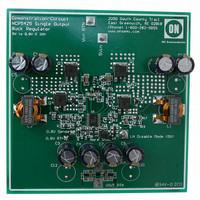
EVAL BOARD FOR NCP5425SO
Manufacturer
ON Semiconductor
Specifications of NCP5425SOEVB
Design Resources
NCP5425SOEVB BOM NCP5425SOEVB Gerber Files NCP5425SOEVB Schematic
Main Purpose
DC/DC, Step Down
Outputs And Type
1, Non-Isolated
Voltage - Output
0.8V
Current - Output
30A
Voltage - Input
4.6 ~ 12 V
Regulator Topology
Buck
Frequency - Switching
300kHz
Board Type
Fully Populated
Utilized Ic / Part
NCP5425
Lead Free Status / RoHS Status
Lead free / RoHS Compliant
Power - Output
-
Lead Free Status / Rohs Status
Lead free / RoHS Compliant
For Use With/related Products
NCP5425SO
Other names
NCP5425SOEVBOS


PIN FUNCTION DESCRIPTION
Pin No.
10
12
13
14
15
16
17
18
19
20
11
1
2
3
4
5
6
7
8
9
GATE(H)1
GATE(H)2
GATE(L)1
GATE(L)2
Symbol
COMP1
COMP2
MODE
V
R
GND
IS+1
IS−1
V
V
IS+2
IS−2
BST
V
NC
NC
REF2
OSC
FB1
FB2
CC
High Side Switch FET driver pin for the channel 1 FET.
Low Side Synchronous FET driver pin for the channel 1 FET.
Ground. All circuits are referenced to this pin. IC substrate connection.
Power input for GATE(H)1 and GATE(H)2 pins.
No connection.
No connection.
Positive input for channel 1 overcurrent comparator.
Negative input for channel 1 overcurrent comparator.
Error amplifier inverting input for channel 1.
Channel 1 Error Amp output. PWM comparator reference input. A capacitor to GND provides Error
Amp compensation. The same capacitor provides soft−start timing for channel 1. This pin also disables
the channel 1 output when pulled below 0.2 V.
Channel 2 Error Amp output. PWM comparator reference input. A capacitor to GND provides Error
Amp compensation and soft−start timing for channel 2. Channel 2 output is disabled when this pin is
pulled below 0.2 V.
Error amplifier inverting input for channel 2.
Error amplifier noninverting input for channel 2.
Positive input for channel 2 overcurrent comparator.
Negative input for channel 2 overcurrent comparator.
Input pin used to inform internal circuitry of dual output or single output operation. Ground this pin for
dual output operation, leave open for single output operation.
A resistor from this pin to ground sets switching frequency.
Input Power supply pin. Power input for GATE(L)1 and GATE(L)2 pins.
Low Side Synchronous FET driver pin for the channel 2 FET.
High Side Switch FET driver pin for the channel 2 FET.
http://onsemi.com
NCP5425
6
Description
Related parts for NCP5425SOEVB
Image
Part Number
Description
Manufacturer
Datasheet
Request
R

Part Number:
Description:
Dual Synchronous Buck Controller
Manufacturer:
ON Semiconductor
Datasheet:
Part Number:
Description:
ON Semiconductor [VOLTAGE REGULATOR]
Manufacturer:
ON Semiconductor
Datasheet:
Part Number:
Description:
357-036-542-201 CARDEDGE 36POS DL .156 BLK LOPRO
Manufacturer:
ON Semiconductor
Datasheet:
Part Number:
Description:
357-036-542-201 CARDEDGE 36POS DL .156 BLK LOPRO
Manufacturer:
ON Semiconductor
Datasheet:
Part Number:
Description:
357-036-542-201 CARDEDGE 36POS DL .156 BLK LOPRO
Manufacturer:
ON Semiconductor
Datasheet:
Part Number:
Description:
357-036-542-201 CARDEDGE 36POS DL .156 BLK LOPRO
Manufacturer:
ON Semiconductor
Datasheet:
Part Number:
Description:
357-036-542-201 CARDEDGE 36POS DL .156 BLK LOPRO
Manufacturer:
ON Semiconductor
Datasheet:
Part Number:
Description:
357-036-542-201 CARDEDGE 36POS DL .156 BLK LOPRO
Manufacturer:
ON Semiconductor
Datasheet:
Part Number:
Description:
357-036-542-201 CARDEDGE 36POS DL .156 BLK LOPRO
Manufacturer:
ON Semiconductor
Datasheet:
Part Number:
Description:
357-036-542-201 CARDEDGE 36POS DL .156 BLK LOPRO
Manufacturer:
ON Semiconductor
Datasheet:
Part Number:
Description:
357-036-542-201 CARDEDGE 36POS DL .156 BLK LOPRO
Manufacturer:
ON Semiconductor
Datasheet:
Part Number:
Description:
357-036-542-201 CARDEDGE 36POS DL .156 BLK LOPRO
Manufacturer:
ON Semiconductor
Datasheet:
Part Number:
Description:
Manufacturer:
ON Semiconductor
Datasheet:
Part Number:
Description:
Manufacturer:
ON Semiconductor
Datasheet: