NCP3063DIPINVEVB ON Semiconductor, NCP3063DIPINVEVB Datasheet - Page 10
NCP3063DIPINVEVB
Manufacturer Part Number
NCP3063DIPINVEVB
Description
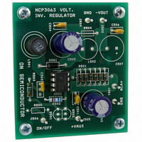
EVAL BOARD FOR NCP3063DIPINV
Manufacturer
ON Semiconductor
Specifications of NCP3063DIPINVEVB
Design Resources
NCP3063DIPINVEVB BOM NCP3063DIPINVEVB Gerbers NCP3063 EVB Schematic
Main Purpose
DC/DC, Negative Inverter
Outputs And Type
1, Non-Isolated
Voltage - Output
-12V
Voltage - Input
4.5 ~ 6 V
Regulator Topology
Inverting
Frequency - Switching
250kHz
Board Type
Fully Populated
Utilized Ic / Part
NCP3063
Lead Free Status / RoHS Status
Lead free / RoHS Compliant
Current - Output
-
Power - Output
-
Lead Free Status / Rohs Status
Lead free / RoHS Compliant
For Use With/related Products
NCP3063DIPINV
Other names
NCP3063DIPINVEVBOS


Value of Components
Test Results
Name
L201
D201
C202
C205
C203
Line Regulation
Load Regulation
Output Ripple
Efficiency
Short Circuit Current
+V
IN
J202
J201
GND
= +12 V
1
1
0.1 mF
Figure 17. Buck Demoboard Layout
C201
Test
Value
47 mH, I
1 A, 40 V Schottky Rectifier
220 mF, 50 V, Low ESR
470 mF, 25 V, Low ESR
2.2 nF Ceramic Capacitor
sat
+
> 1.5 A
220 mF / 50 V
R201
0R15
C202
V
V
V
V
V
in
in
in
in
in
= 9 V to 12 V, I
= 12 V, I
= 12 V, I
= 12 V, I
= 12 V, R
Figure 16. Typical Buck Application Schematic
8
7
6
5
R202
2K4 ±1%
o
o
o
N.C.
COMP
I
V
load
PK
= 80 mA to 800 mA
= 40 mA to 800 mA
= 400 mA to 800 mA
CC
NCP3063
U201
= 0.15 W
o
TCAP
= 800 mA
SWC
SWE
GND
http://onsemi.com
1
2
3
4
3K9 ±1%
Condition
R203
10
C203
2.2 nF
Figure 18. Efficiency vs. Output Current for the Buck
76
74
72
70
68
66
64
Name
R201
R202
R203
C201
C202
Demo Board at V
0.1 0.2
L201
1N5819
D201
0.3
47 mH
Value
150 mW, 0.5 W
2.40 kW
3.90 kW
100 nF Ceramic Capacitor
100 nF Ceramic Capacitor
C206
0.1 mF
0.4
OUTPUT LOAD (Adc)
in
= 12 V, V
0.5
+
470 mF / 25 V
C205
8 mV
9 mV
≤ 85 mV
> 73%
1.25 A
0.6
out
+V
= 3.3 V, T
pp
OUT
0.7
Results
= +3.3 V / 800 mA
0.8
J204
J203
GND
A
1
1
= 255C
0.9
1.0
Related parts for NCP3063DIPINVEVB
Image
Part Number
Description
Manufacturer
Datasheet
Request
R

Part Number:
Description:
1.5 A, Step−Up/Down/Inverting Switching Regulators
Manufacturer:
ONSEMI [ON Semiconductor]
Datasheet:

Part Number:
Description:
EVAL BOARD FOR NCP3063DFBSTG
Manufacturer:
ON Semiconductor
Datasheet:

Part Number:
Description:
EVAL BOARD FOR NCP3063DIPBCK
Manufacturer:
ON Semiconductor
Datasheet:

Part Number:
Description:
EVAL BOARD FOR NCP3063SMDBST
Manufacturer:
ON Semiconductor
Datasheet:

Part Number:
Description:
EVAL BOARD FOR NCP3063SMINVG
Manufacturer:
ON Semiconductor
Datasheet:

Part Number:
Description:
EVAL BOARD FOR NCP3063BSTEXG
Manufacturer:
ON Semiconductor
Datasheet:

Part Number:
Description:
ON Semiconductor [VOLTAGE REGULATOR]
Manufacturer:
ON Semiconductor
Datasheet:
Part Number:
Description:
357-036-542-201 CARDEDGE 36POS DL .156 BLK LOPRO
Manufacturer:
ON Semiconductor
Datasheet:
Part Number:
Description:
357-036-542-201 CARDEDGE 36POS DL .156 BLK LOPRO
Manufacturer:
ON Semiconductor
Datasheet:
Part Number:
Description:
357-036-542-201 CARDEDGE 36POS DL .156 BLK LOPRO
Manufacturer:
ON Semiconductor
Datasheet:
Part Number:
Description:
357-036-542-201 CARDEDGE 36POS DL .156 BLK LOPRO
Manufacturer:
ON Semiconductor
Datasheet:
Part Number:
Description:
357-036-542-201 CARDEDGE 36POS DL .156 BLK LOPRO
Manufacturer:
ON Semiconductor
Datasheet:
Part Number:
Description:
357-036-542-201 CARDEDGE 36POS DL .156 BLK LOPRO
Manufacturer:
ON Semiconductor
Datasheet:
Part Number:
Description:
357-036-542-201 CARDEDGE 36POS DL .156 BLK LOPRO
Manufacturer:
ON Semiconductor
Datasheet:
Part Number:
Description:
357-036-542-201 CARDEDGE 36POS DL .156 BLK LOPRO
Manufacturer:
ON Semiconductor
Datasheet: