NCP3063DIPINVEVB ON Semiconductor, NCP3063DIPINVEVB Datasheet - Page 3
NCP3063DIPINVEVB
Manufacturer Part Number
NCP3063DIPINVEVB
Description
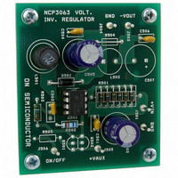
EVAL BOARD FOR NCP3063DIPINV
Manufacturer
ON Semiconductor
Specifications of NCP3063DIPINVEVB
Design Resources
NCP3063DIPINVEVB BOM NCP3063DIPINVEVB Gerbers NCP3063 EVB Schematic
Main Purpose
DC/DC, Negative Inverter
Outputs And Type
1, Non-Isolated
Voltage - Output
-12V
Voltage - Input
4.5 ~ 6 V
Regulator Topology
Inverting
Frequency - Switching
250kHz
Board Type
Fully Populated
Utilized Ic / Part
NCP3063
Lead Free Status / RoHS Status
Lead free / RoHS Compliant
Current - Output
-
Power - Output
-
Lead Free Status / Rohs Status
Lead free / RoHS Compliant
For Use With/related Products
NCP3063DIPINV
Other names
NCP3063DIPINVEVBOS


Stresses exceeding Maximum Ratings may damage the device. Maximum Ratings are stress ratings only. Functional operation above the
Recommended Operating Conditions is not implied. Extended exposure to stresses above the Recommended Operating Conditions may affect
device reliability.
1. This device series contains ESD protection and exceeds the following tests:
2. This device contains latch−up protection and exceeds 100 mA per JEDEC Standard JESD78.
3. The relation between junction temperature, ambient temperature and Total Power dissipated in IC is T
4. The pins which are not defined may not be loaded by external signals
PIN DESCRIPTION
MAXIMUM RATINGS
Timing Capacitor Pin 3
DFN−8
POWER DISSIPATION AND THERMAL CHARACTERISTICS
V
Comparator Inverting Input pin 5
Darlington Switch Collector pin 1
Darlington Switch Emitter pin 2 (transistor OFF)
Darlington Switch Collector to Emitter pin 1−2
Darlington Switch Current
I
PDIP−8
SOIC−8
Storage Temperature Range
Maximum Junction Temperature
Operating Junction Temperature Range (Note 3)
Exposed
Pin No.
pk
CC
Pad
Sense Pin 7
Pin 1−8: Human Body Model 2000 V per AEC Q100−002; 003 or JESD22/A114; A115
Machine Model Method 200 V
1
2
3
4
5
6
7
8
pin 6
Timing Capacitor
Switch Collector
Oscillator Input
Switch Emitter
Inverting Input
Exposed Pad
Comparator
Pin Name
I
pk
GND
N.C.
V
Sense
CC
(measured vs. Pin 4, unless otherwise noted)
Thermal Resistance, Junction−to−Case
Rating
Rating
Thermal Resistance, Junction−to−Air
Thermal Resistance, Junction−to−Air
Thermal Resistance, Junction−to−Air
Internal Darlington switch collector
Internal Darlington switch emitter
Timing Capacitor
Ground pin for all internal circuits
Inverting input pin of internal comparator
Voltage Supply
Peak Current Sense Input to monitor the voltage drop across an external resistor to limit the peak
current through the circuit
Pin Not Connected
The exposed pad beneath the package must be connected to GND (Pin 4). Additionally, using
proper layout techniques, the exposed pad can greatly enhance the power dissipation capabilities
of the NCP3063.
NCP3063B, NCV3063
http://onsemi.com
NCP3063
3
Symbol
Symbol
V
T
V
V
V
T
R
R
R
R
V
V
SWCE
J MAX
V
I
TCAP
Description
SWC
SWE
SW
STG
T
qJC
IPK
qJA
qJA
qJA
CC
CII
J
−0.2 to V
−0.2 to + V
−0.6 to + V
−0.2 to +1.4
−65 to +150
−40 to +125
0 to +40
0 to +40
0 to +40
0 to +70
Value
Value
+150
J
100
180
1.5
45
80
= T
CC
A
+ 0.2
CC
CC
+ R
q •
P
D
°C/W
°C/W
°C/W
Unit
Unit
°C
°C
°C
V
V
V
V
V
A
V
V
Related parts for NCP3063DIPINVEVB
Image
Part Number
Description
Manufacturer
Datasheet
Request
R

Part Number:
Description:
1.5 A, Step−Up/Down/Inverting Switching Regulators
Manufacturer:
ONSEMI [ON Semiconductor]
Datasheet:

Part Number:
Description:
EVAL BOARD FOR NCP3063DFBSTG
Manufacturer:
ON Semiconductor
Datasheet:

Part Number:
Description:
EVAL BOARD FOR NCP3063DIPBCK
Manufacturer:
ON Semiconductor
Datasheet:

Part Number:
Description:
EVAL BOARD FOR NCP3063SMDBST
Manufacturer:
ON Semiconductor
Datasheet:

Part Number:
Description:
EVAL BOARD FOR NCP3063SMINVG
Manufacturer:
ON Semiconductor
Datasheet:

Part Number:
Description:
EVAL BOARD FOR NCP3063BSTEXG
Manufacturer:
ON Semiconductor
Datasheet:

Part Number:
Description:
ON Semiconductor [VOLTAGE REGULATOR]
Manufacturer:
ON Semiconductor
Datasheet:
Part Number:
Description:
357-036-542-201 CARDEDGE 36POS DL .156 BLK LOPRO
Manufacturer:
ON Semiconductor
Datasheet:
Part Number:
Description:
357-036-542-201 CARDEDGE 36POS DL .156 BLK LOPRO
Manufacturer:
ON Semiconductor
Datasheet:
Part Number:
Description:
357-036-542-201 CARDEDGE 36POS DL .156 BLK LOPRO
Manufacturer:
ON Semiconductor
Datasheet:
Part Number:
Description:
357-036-542-201 CARDEDGE 36POS DL .156 BLK LOPRO
Manufacturer:
ON Semiconductor
Datasheet:
Part Number:
Description:
357-036-542-201 CARDEDGE 36POS DL .156 BLK LOPRO
Manufacturer:
ON Semiconductor
Datasheet:
Part Number:
Description:
357-036-542-201 CARDEDGE 36POS DL .156 BLK LOPRO
Manufacturer:
ON Semiconductor
Datasheet:
Part Number:
Description:
357-036-542-201 CARDEDGE 36POS DL .156 BLK LOPRO
Manufacturer:
ON Semiconductor
Datasheet:
Part Number:
Description:
357-036-542-201 CARDEDGE 36POS DL .156 BLK LOPRO
Manufacturer:
ON Semiconductor
Datasheet: