NCP3063DIPINVEVB ON Semiconductor, NCP3063DIPINVEVB Datasheet - Page 5
NCP3063DIPINVEVB
Manufacturer Part Number
NCP3063DIPINVEVB
Description
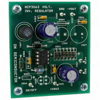
EVAL BOARD FOR NCP3063DIPINV
Manufacturer
ON Semiconductor
Specifications of NCP3063DIPINVEVB
Design Resources
NCP3063DIPINVEVB BOM NCP3063DIPINVEVB Gerbers NCP3063 EVB Schematic
Main Purpose
DC/DC, Negative Inverter
Outputs And Type
1, Non-Isolated
Voltage - Output
-12V
Voltage - Input
4.5 ~ 6 V
Regulator Topology
Inverting
Frequency - Switching
250kHz
Board Type
Fully Populated
Utilized Ic / Part
NCP3063
Lead Free Status / RoHS Status
Lead free / RoHS Compliant
Current - Output
-
Power - Output
-
Lead Free Status / Rohs Status
Lead free / RoHS Compliant
For Use With/related Products
NCP3063DIPINV
Other names
NCP3063DIPINVEVBOS


450
400
350
300
250
200
150
100
2.4
2.2
2.0
1.8
1.6
1.4
1.2
1.0
2.0
1.9
1.8
1.7
1.6
1.5
1.4
1.3
1.2
1.1
1.0
50
0
Darlington Switch Voltage Drop vs. Emitter Current
−50
0 1 2 3 4 5 6 7 8 9 10 11 12 1314 1516 1718 1920
Darlington Switch Voltage Drop vs. Temperature
Figure 7. Emitter Follower Configuration Output
0
Figure 9. Emitter Follower Configuration Output
Figure 5. Oscillator Frequency vs. Oscillator
V
T
J
CC
= 25°C
= 5.0 V
T
J
, JUNCTION TEMPERATURE (°C)
0
I
E
Ct, CAPACITANCE (nF)
, EMITTER CURRENT (A)
Timing Capacitor
0.5
50
1.0
V
I
E
100
CC
= 1 A
= 5.0 V
http://onsemi.com
150
1.5
5
1.25
1.20
1.15
1.10
1.05
190
180
170
160
150
140
130
120
110
1.0
1.5
1.4
1.3
1.2
1.1
1.0
0.9
0.8
0.7
0.6
0.5
−50
3
0
Figure 8. Common Emitter Configuration Output
Darlington Switch Voltage Drop vs. Temperature
Output Darlington Switch Voltage Drop vs.
Figure 6. Oscillator Frequency vs. Supply
Figure 10. Common Emitter Configuration
7
T
J
12
, JUNCTION TEMPERATURE (°C)
I
C
0
V
, COLLECTOR CURRENT (A)
CC
0.5
, SUPPLY VOLTAGE (V)
Collector Current
16
Voltage
21
50
25
1.0
29
V
I
100
C
V
T
CC
J
C
T
CC
= 1 A
J
= 25°C
T
= 5.0 V
= 25°C
34
= 5.0 V
= 2.2 nF
38
150
1.5
40
Related parts for NCP3063DIPINVEVB
Image
Part Number
Description
Manufacturer
Datasheet
Request
R

Part Number:
Description:
1.5 A, Step−Up/Down/Inverting Switching Regulators
Manufacturer:
ONSEMI [ON Semiconductor]
Datasheet:

Part Number:
Description:
EVAL BOARD FOR NCP3063DFBSTG
Manufacturer:
ON Semiconductor
Datasheet:

Part Number:
Description:
EVAL BOARD FOR NCP3063DIPBCK
Manufacturer:
ON Semiconductor
Datasheet:

Part Number:
Description:
EVAL BOARD FOR NCP3063SMDBST
Manufacturer:
ON Semiconductor
Datasheet:

Part Number:
Description:
EVAL BOARD FOR NCP3063SMINVG
Manufacturer:
ON Semiconductor
Datasheet:

Part Number:
Description:
EVAL BOARD FOR NCP3063BSTEXG
Manufacturer:
ON Semiconductor
Datasheet:

Part Number:
Description:
ON Semiconductor [VOLTAGE REGULATOR]
Manufacturer:
ON Semiconductor
Datasheet:
Part Number:
Description:
357-036-542-201 CARDEDGE 36POS DL .156 BLK LOPRO
Manufacturer:
ON Semiconductor
Datasheet:
Part Number:
Description:
357-036-542-201 CARDEDGE 36POS DL .156 BLK LOPRO
Manufacturer:
ON Semiconductor
Datasheet:
Part Number:
Description:
357-036-542-201 CARDEDGE 36POS DL .156 BLK LOPRO
Manufacturer:
ON Semiconductor
Datasheet:
Part Number:
Description:
357-036-542-201 CARDEDGE 36POS DL .156 BLK LOPRO
Manufacturer:
ON Semiconductor
Datasheet:
Part Number:
Description:
357-036-542-201 CARDEDGE 36POS DL .156 BLK LOPRO
Manufacturer:
ON Semiconductor
Datasheet:
Part Number:
Description:
357-036-542-201 CARDEDGE 36POS DL .156 BLK LOPRO
Manufacturer:
ON Semiconductor
Datasheet:
Part Number:
Description:
357-036-542-201 CARDEDGE 36POS DL .156 BLK LOPRO
Manufacturer:
ON Semiconductor
Datasheet:
Part Number:
Description:
357-036-542-201 CARDEDGE 36POS DL .156 BLK LOPRO
Manufacturer:
ON Semiconductor
Datasheet: