LM2594APDBCKGEVB ON Semiconductor, LM2594APDBCKGEVB Datasheet - Page 16
LM2594APDBCKGEVB
Manufacturer Part Number
LM2594APDBCKGEVB
Description
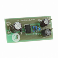
EVAL BOARD FOR LM2594APDBCKG
Manufacturer
ON Semiconductor
Specifications of LM2594APDBCKGEVB
Design Resources
LM2594APDBCKGEVB BOM LM2594APDBCKGEVB Schematic LM2594APDBCKGEVB Gerber Files
Main Purpose
DC/DC, Step Down
Outputs And Type
1, Non-Isolated
Voltage - Output
5V
Current - Output
500mA
Voltage - Input
4.5 ~ 40 V
Regulator Topology
Buck
Frequency - Switching
150kHz
Board Type
Fully Populated
Utilized Ic / Part
LM2594
Lead Free Status / RoHS Status
Lead free / RoHS Compliant
Power - Output
-
Lead Free Status / Rohs Status
Lead free / RoHS Compliant
For Use With/related Products
LM2594APDBCKG
Other names
LM2594ADPBCKGEVB
LM2594ADPBCKGEVBOS
LM2594APDBCKGEVBOS
LM2594ADPBCKGEVBOS
LM2594APDBCKGEVBOS


interference between two or more of the regulator circuits,
especially at high currents due to mutual coupling. A toroid,
pot core or E−core (closed magnetic structure) should be
used in such applications.
Do Not Operate an Inductor Beyond its
Maximum Rated Current
cause the inductor to overheat because of the copper wire
losses, or the core may saturate. Core saturation occurs when
the flux density is too high and consequently the cross
sectional area of the core can no longer support additional
lines of magnetic flux.
inductance value decreases rapidly and the inductor begins
to look mainly resistive. It has only the DC resistance of the
winding. This can cause the switch current to rise very
rapidly and force the LM2594 internal switch into
cycle−by−cycle current limit, thus reducing the DC output
load current. This can also result in overheating of the
Output Voltage Ripple and Transients
Source of the Output Ripple
regulator, its output voltage, if left unfiltered, will contain a
sawtooth ripple voltage at the switching frequency. The
output ripple voltage value ranges from 0.5% to 3% of the
output voltage. It is caused mainly by the inductor sawtooth
ripple current multiplied by the ESR of the output capacitor.
Short Voltage Spikes and How to Reduce Them
voltage spikes at the peaks of the sawtooth waveform (see
Figure 22). These voltage spikes are present because of the
fast switching action of the output switch, and the parasitic
inductance of the output filter capacitor. There are some
other important factors such as wiring inductance, stray
capacitance, as well as the scope probe used to evaluate these
transients, all these contribute to the amplitude of these
spikes. To minimize these voltage spikes, low inductance
capacitors should be used, and their lead lengths must be
kept short. The importance of quality printed circuit board
layout design should also be highlighted.
Unfiltered
Exceeding an inductor’s maximum current rating may
This causes the permeability of the core to drop, the
Since the LM2594 is a switch mode power supply
The regulator output voltage may also contain short
Filtered
Voltage
Voltage
Output
Output
Figure 22. Output Ripple Voltage Waveforms
HORIZONTAL TIME BASE: 5.0 ms/DIV
GENERAL RECOMMENDATIONS
Voltage spikes
caused by
switching action
of the output
switch and the
parasitic
inductance of the
output capacitor
http://onsemi.com
16
inductor and/or the LM2594. Different inductor types have
different saturation characteristics, and this should be kept
in mind when selecting an inductor.
Minimizing the Output Ripple
to enlarge the inductance value of the inductor L1 and/or to
use a larger value output capacitor. There is also another way
to smooth the output by means of an additional LC filter (3 mH,
100 mF), that can be added to the output (see Figure 31) to
further reduce the amount of output ripple and transients.
With such a filter it is possible to reduce the output ripple
voltage transients 10 times or more. Figure 22 shows the
difference between filtered and unfiltered output waveforms
of the regulator shown in Figure 31.
of the converter, while the upper waveform shows the output
ripple voltage filtered by an additional LC filter.
Heatsinking and Thermal Considerations
packages. When used in the typical application the copper
lead frame conducts the majority of the heat from the die,
through the leads, to the printed circuit copper. The copper
and the board are the heatsink for this package and the other
heat producing components, such as the catch diode and
inductor. For the best thermal performance, wide copper
traces should be used and all ground and unused pins should
be soldered to generous amounts of printed circuit board
copper, such as a ground plane. Large areas of copper
provide the best transfer of heat to the surrounding air. One
exception to this is the output (switch) pin, which should not
have large areas of copper in order to minimize coupling to
sensitive circuitry.
achieved even by using of double sided or multilayer boards
which can provide even better heat path to the ambient.
Using a socket for the 8−pin DIP package is not
recommended because socket represents an additional
thermal resistance, and as a result the junction temperature
will be higher.
Waveform
Waveform
Inductor
In order to minimize the output ripple voltage it is possible
The lower waveform is from the normal unfiltered output
The LM2574 is available in both 8−pin DIP and SOIC−8
Additional improvement in heat dissipation can be
Current
Current
Figure 21. Discontinuous Mode Switching Current
Switch
Power
0.05 A
0.05 A
0 A
0 A
HORIZONTAL TIME BASE: 2.0 ms/DIV
Waveforms
Related parts for LM2594APDBCKGEVB
Image
Part Number
Description
Manufacturer
Datasheet
Request
R

Part Number:
Description:
ON Semiconductor [VOLTAGE REGULATOR]
Manufacturer:
ON Semiconductor
Datasheet:
Part Number:
Description:
357-036-542-201 CARDEDGE 36POS DL .156 BLK LOPRO
Manufacturer:
ON Semiconductor
Datasheet:
Part Number:
Description:
357-036-542-201 CARDEDGE 36POS DL .156 BLK LOPRO
Manufacturer:
ON Semiconductor
Datasheet:
Part Number:
Description:
357-036-542-201 CARDEDGE 36POS DL .156 BLK LOPRO
Manufacturer:
ON Semiconductor
Datasheet:
Part Number:
Description:
357-036-542-201 CARDEDGE 36POS DL .156 BLK LOPRO
Manufacturer:
ON Semiconductor
Datasheet:
Part Number:
Description:
357-036-542-201 CARDEDGE 36POS DL .156 BLK LOPRO
Manufacturer:
ON Semiconductor
Datasheet:
Part Number:
Description:
357-036-542-201 CARDEDGE 36POS DL .156 BLK LOPRO
Manufacturer:
ON Semiconductor
Datasheet:
Part Number:
Description:
357-036-542-201 CARDEDGE 36POS DL .156 BLK LOPRO
Manufacturer:
ON Semiconductor
Datasheet:
Part Number:
Description:
357-036-542-201 CARDEDGE 36POS DL .156 BLK LOPRO
Manufacturer:
ON Semiconductor
Datasheet:
Part Number:
Description:
357-036-542-201 CARDEDGE 36POS DL .156 BLK LOPRO
Manufacturer:
ON Semiconductor
Datasheet:
Part Number:
Description:
357-036-542-201 CARDEDGE 36POS DL .156 BLK LOPRO
Manufacturer:
ON Semiconductor
Datasheet:
Part Number:
Description:
Manufacturer:
ON Semiconductor
Datasheet:
Part Number:
Description:
Manufacturer:
ON Semiconductor
Datasheet:
Part Number:
Description:
Manufacturer:
ON Semiconductor
Datasheet: