LM2594APDBCKGEVB ON Semiconductor, LM2594APDBCKGEVB Datasheet - Page 20
LM2594APDBCKGEVB
Manufacturer Part Number
LM2594APDBCKGEVB
Description
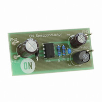
EVAL BOARD FOR LM2594APDBCKG
Manufacturer
ON Semiconductor
Specifications of LM2594APDBCKGEVB
Design Resources
LM2594APDBCKGEVB BOM LM2594APDBCKGEVB Schematic LM2594APDBCKGEVB Gerber Files
Main Purpose
DC/DC, Step Down
Outputs And Type
1, Non-Isolated
Voltage - Output
5V
Current - Output
500mA
Voltage - Input
4.5 ~ 40 V
Regulator Topology
Buck
Frequency - Switching
150kHz
Board Type
Fully Populated
Utilized Ic / Part
LM2594
Lead Free Status / RoHS Status
Lead free / RoHS Compliant
Power - Output
-
Lead Free Status / Rohs Status
Lead free / RoHS Compliant
For Use With/related Products
LM2594APDBCKG
Other names
LM2594ADPBCKGEVB
LM2594ADPBCKGEVBOS
LM2594APDBCKGEVBOS
LM2594ADPBCKGEVBOS
LM2594APDBCKGEVBOS


Delayed Startup
already mentioned above, which require a higher amount of
startup current. In such cases, if the input power source is
limited, this delayed startup feature becomes very useful.
voltage is applied and the time when the output voltage
comes up, the circuit in Figure 28 can be used. As the input
voltage is applied, the capacitor C1 charges up, and the
voltage across the resistor R2 falls down. When the voltage
on the ON/OFF pin falls below the threshold value 1.3 V, the
regulator starts up. Resistor R1 is included to limit the
maximum voltage applied to the ON/OFF pin. It reduces the
power supply noise sensitivity, and also limits the capacitor
C1 discharge current, but its use is not mandatory.
respectively) ripple voltage exists, a long delay time can
cause some problems by coupling the ripple into the
ON/OFF pin, the regulator could be switched periodically
on and off with the line (or double) frequency.
Undervoltage Lockout
the input voltage reaches a certain threshold level. Figure 29
shows an undervoltage lockout circuit applied to a buck
regulator. A version of this circuit for buck−boost converter
is shown in Figure 30. Resistor R3 pulls the ON/OFF pin
high and keeps the regulator off until the input voltage
reaches a predetermined threshold level with respect to the
ground Pin 3, which is determined by the following
expression:
There are some applications, like the inverting regulator
To provide a time delay between the time when the input
When a high 50 Hz or 60 Hz (100 Hz or 120 Hz
Some applications require the regulator to remain off until
NOTE: This picture does not show the complete circuit.
100 mF
+V
Figure 28. Delayed Startup Circuitry
in
V
C
in
th
[ V
Z1
) 1.0 ) R2
C1
0.1 mF
47 k
R1
+V
in
7
R1
5
ON/OFF
R2
47 k
LM2594
V
BE
( Q1 )
6
GN
D
http://onsemi.com
20
current:
conditions, the worst case occurs when V
Adjustable Output, Low−Ripple Power Supply
features an adjustable output voltage is shown in Figure 31.
The input voltage ranges from roughly 3.0 V to 40 V. In order
to achieve a 10 or more times reduction of output ripple, an
additional L−C filter is included in this circuit.
where t on +
The following formula is used to obtain the peak inductor
Under normal continuous inductor current operating
A 0.5 A output current capability power supply that
This regulator delivers 0.5 A into 1.2 V to 35 V output.
1N5242B
1N5242B
NOTE: This picture does not show the complete circuit.
NOTE: This picture does not show the complete circuit.
Figure 29. Undervoltage Lockout Circuit for
+V
Figure 30. Undervoltage Lockout Circuit for
15 k
15 k
I
R2
Z1
R1
+V
in
10 k
10 k
peak
R2
Z1
R1
in
47 k
[
V
R3
47 k
R3
in
Buck−Boost Converter
I
Load
|V
Q1
2N3904
) |V
Buck Converter
Q1
2N3904
O
|
(V
O
V
in
|
C
100 mF
in
+V
x 1.0
in
C
100 mF
) |V
+V
in
in
f osc
7
in
7
5
O
, and f osc + 52 kHz.
5
|)
ON/OFF
LM2594
V
)
ON/OFF
LM2594
th
≈ 13 V
in
V
is minimal.
in
6
2L 1
x t on
6
GN
D
V
GN
D
th
≈ 13 V
V
out
Related parts for LM2594APDBCKGEVB
Image
Part Number
Description
Manufacturer
Datasheet
Request
R

Part Number:
Description:
ON Semiconductor [VOLTAGE REGULATOR]
Manufacturer:
ON Semiconductor
Datasheet:
Part Number:
Description:
357-036-542-201 CARDEDGE 36POS DL .156 BLK LOPRO
Manufacturer:
ON Semiconductor
Datasheet:
Part Number:
Description:
357-036-542-201 CARDEDGE 36POS DL .156 BLK LOPRO
Manufacturer:
ON Semiconductor
Datasheet:
Part Number:
Description:
357-036-542-201 CARDEDGE 36POS DL .156 BLK LOPRO
Manufacturer:
ON Semiconductor
Datasheet:
Part Number:
Description:
357-036-542-201 CARDEDGE 36POS DL .156 BLK LOPRO
Manufacturer:
ON Semiconductor
Datasheet:
Part Number:
Description:
357-036-542-201 CARDEDGE 36POS DL .156 BLK LOPRO
Manufacturer:
ON Semiconductor
Datasheet:
Part Number:
Description:
357-036-542-201 CARDEDGE 36POS DL .156 BLK LOPRO
Manufacturer:
ON Semiconductor
Datasheet:
Part Number:
Description:
357-036-542-201 CARDEDGE 36POS DL .156 BLK LOPRO
Manufacturer:
ON Semiconductor
Datasheet:
Part Number:
Description:
357-036-542-201 CARDEDGE 36POS DL .156 BLK LOPRO
Manufacturer:
ON Semiconductor
Datasheet:
Part Number:
Description:
357-036-542-201 CARDEDGE 36POS DL .156 BLK LOPRO
Manufacturer:
ON Semiconductor
Datasheet:
Part Number:
Description:
357-036-542-201 CARDEDGE 36POS DL .156 BLK LOPRO
Manufacturer:
ON Semiconductor
Datasheet:
Part Number:
Description:
Manufacturer:
ON Semiconductor
Datasheet:
Part Number:
Description:
Manufacturer:
ON Semiconductor
Datasheet:
Part Number:
Description:
Manufacturer:
ON Semiconductor
Datasheet: