LM2594APDBCKGEVB ON Semiconductor, LM2594APDBCKGEVB Datasheet - Page 2
LM2594APDBCKGEVB
Manufacturer Part Number
LM2594APDBCKGEVB
Description
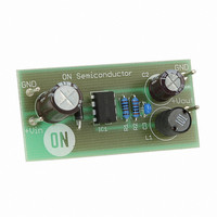
EVAL BOARD FOR LM2594APDBCKG
Manufacturer
ON Semiconductor
Specifications of LM2594APDBCKGEVB
Design Resources
LM2594APDBCKGEVB BOM LM2594APDBCKGEVB Schematic LM2594APDBCKGEVB Gerber Files
Main Purpose
DC/DC, Step Down
Outputs And Type
1, Non-Isolated
Voltage - Output
5V
Current - Output
500mA
Voltage - Input
4.5 ~ 40 V
Regulator Topology
Buck
Frequency - Switching
150kHz
Board Type
Fully Populated
Utilized Ic / Part
LM2594
Lead Free Status / RoHS Status
Lead free / RoHS Compliant
Power - Output
-
Lead Free Status / Rohs Status
Lead free / RoHS Compliant
For Use With/related Products
LM2594APDBCKG
Other names
LM2594ADPBCKGEVB
LM2594ADPBCKGEVBOS
LM2594APDBCKGEVBOS
LM2594ADPBCKGEVBOS
LM2594APDBCKGEVBOS


PIN FUNCTION DESCRIPTION
Pin No.
1 − 3
4
5
6
7
8
C
IN
= 68 mF
12 V
Unregulated
DC Input
OUTPUT
ON/OFF
Symbol
GND
+V
NC
FB
IN
Not Connected
This pin is the direct input of the error amplifier and the resistor network R2, R1 is connected externally to
allow programming of the output voltage.
Allows the switching regulator circuit to be shut down using logic levels, thus dropping the total input supply
current to approximately 50 mA. The threshold voltage is typical. 1.6 V. Applying a voltage above this value
(up to V
the regulator will be in the “on” condition.
Circuit ground pin. See the information about the printed circuit board layout.
Positive input supply for LM2594 step−down switching regulator. In order to minimize voltage transients and
to supply the switching currents needed by the regulator, a suitable input bypass capacitor must be present
(C
Emitter of the internal switch. The saturation voltage Vsat of the output switch is typically 1 V. It should be
kept in mind that PCB area connected to this pin should be kept to a minimum in order to minimize coupling
to sensitive circuitry
IN
+V
in Figure 1)
IN
IN
7
) shuts the regulator off. If the voltage applied to this pin is lower than 1.6 V or if this pin is left open,
Figure 2. Representative Block Diagram
5
ON/OFF
LM2594
Figure 1. Typical Application
http://onsemi.com
6
GND
Description (Refer to Figure 1)
2
4
8
Feedback
Output
D1
1N5817
100 mH
L1
0.5
C
FF
C
220 mF
OUT
R2 = 3k
R1 = 1 kW
V
OUT
= 5 V; I
load
= 0.5 A
Related parts for LM2594APDBCKGEVB
Image
Part Number
Description
Manufacturer
Datasheet
Request
R

Part Number:
Description:
ON Semiconductor [VOLTAGE REGULATOR]
Manufacturer:
ON Semiconductor
Datasheet:
Part Number:
Description:
357-036-542-201 CARDEDGE 36POS DL .156 BLK LOPRO
Manufacturer:
ON Semiconductor
Datasheet:
Part Number:
Description:
357-036-542-201 CARDEDGE 36POS DL .156 BLK LOPRO
Manufacturer:
ON Semiconductor
Datasheet:
Part Number:
Description:
357-036-542-201 CARDEDGE 36POS DL .156 BLK LOPRO
Manufacturer:
ON Semiconductor
Datasheet:
Part Number:
Description:
357-036-542-201 CARDEDGE 36POS DL .156 BLK LOPRO
Manufacturer:
ON Semiconductor
Datasheet:
Part Number:
Description:
357-036-542-201 CARDEDGE 36POS DL .156 BLK LOPRO
Manufacturer:
ON Semiconductor
Datasheet:
Part Number:
Description:
357-036-542-201 CARDEDGE 36POS DL .156 BLK LOPRO
Manufacturer:
ON Semiconductor
Datasheet:
Part Number:
Description:
357-036-542-201 CARDEDGE 36POS DL .156 BLK LOPRO
Manufacturer:
ON Semiconductor
Datasheet:
Part Number:
Description:
357-036-542-201 CARDEDGE 36POS DL .156 BLK LOPRO
Manufacturer:
ON Semiconductor
Datasheet:
Part Number:
Description:
357-036-542-201 CARDEDGE 36POS DL .156 BLK LOPRO
Manufacturer:
ON Semiconductor
Datasheet:
Part Number:
Description:
357-036-542-201 CARDEDGE 36POS DL .156 BLK LOPRO
Manufacturer:
ON Semiconductor
Datasheet:
Part Number:
Description:
Manufacturer:
ON Semiconductor
Datasheet:
Part Number:
Description:
Manufacturer:
ON Semiconductor
Datasheet:
Part Number:
Description:
Manufacturer:
ON Semiconductor
Datasheet: