LM2594APDBCKGEVB ON Semiconductor, LM2594APDBCKGEVB Datasheet - Page 8
LM2594APDBCKGEVB
Manufacturer Part Number
LM2594APDBCKGEVB
Description
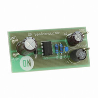
EVAL BOARD FOR LM2594APDBCKG
Manufacturer
ON Semiconductor
Specifications of LM2594APDBCKGEVB
Design Resources
LM2594APDBCKGEVB BOM LM2594APDBCKGEVB Schematic LM2594APDBCKGEVB Gerber Files
Main Purpose
DC/DC, Step Down
Outputs And Type
1, Non-Isolated
Voltage - Output
5V
Current - Output
500mA
Voltage - Input
4.5 ~ 40 V
Regulator Topology
Buck
Frequency - Switching
150kHz
Board Type
Fully Populated
Utilized Ic / Part
LM2594
Lead Free Status / RoHS Status
Lead free / RoHS Compliant
Power - Output
-
Lead Free Status / Rohs Status
Lead free / RoHS Compliant
For Use With/related Products
LM2594APDBCKG
Other names
LM2594ADPBCKGEVB
LM2594ADPBCKGEVBOS
LM2594APDBCKGEVBOS
LM2594ADPBCKGEVBOS
LM2594APDBCKGEVBOS


circuit board is very important. Rapidly switching currents
associated with wiring inductance, stray capacitance and
parasitic inductance of the printed circuit board traces can
generate
electromagnetic interferences (EMI) and affect the desired
operation. As indicated in the Figure 16, to minimize
inductance and ground loops, the length of the leads
indicated by heavy lines should be kept as short as possible.
ground plane construction should be used.
Buck Converter Basics
is the most elementary forward−mode converter. Its basic
schematic can be seen in Figure 17.
time periods. The first one occurs when the series switch is
on, the input voltage is connected to the input of the inductor.
rectifier (or catch diode) is reverse biased. During this
period, since there is a constant voltage source connected
across the inductor, the inductor current begins to linearly
ramp upwards, as described by the following equation:
material in the form of magnetic flux. If the inductor is
properly designed, there is sufficient energy stored to carry
the requirements of the load during the “off” period.
When the power switch turns off, the voltage across the
inductor reverses its polarity and is clamped at one diode
voltage drop below ground by the catch diode. The current
now flows through the catch diode thus maintaining the load
current loop. This removes the stored energy from the
inductor. The inductor current during this time is:
As in any switching regulator, the layout of the printed
For best results, single−point grounding (as indicated) or
The LM2594 is a “Buck” or Step−Down Converter which
The operation of this regulator topology has two distinct
The output of the inductor is the output voltage, and the
During this “on” period, energy is stored within the core
The next period is the “off” period of the power switch.
V
in
voltage
Power
Switch
Figure 17. Basic Buck Converter
I
I
L(on)
L(off)
transients
+
+
D
V
V
IN
OUT
* V
* V
L
L
OUT
L
which
D
t
t
off
on
C
out
can
PCB LAYOUT GUIDELINES
DESIGN PROCEDURE
generate
http://onsemi.com
R
Load
8
(emitter of the internal switch) of the LM2594 should be
kept to a minimum in order to minimize coupling to sensitive
circuitry.
important to keep the sensitive feedback wiring short. To
assure this, physically locate the programming resistors near
to the regulator, when using the adjustable version of the
LM2594 regulator.
turned on. Regulation of the converter is accomplished by
varying the duty cycle of the power switch. It is possible to
describe the duty cycle as follows:
cycle can also be described as:
of the catch diode voltage and the inductor current.
On the other hand, the PCB area connected to the Pin 2
Another sensitive part of the circuit is the feedback. It is
This period ends when the power switch is once again
For the buck converter with ideal components, the duty
Figure 18 shows the buck converter, idealized waveforms
d +
Figure 18. Buck Converter Idealized Waveforms
t on
I
Switch
V
Power
min
Diode
T
D
Off
(FWD)
, where T is the period of switching.
V
on(SW)
Switch
Power
Switch
Power
On
d +
Switch
Power
Diode
Off
V out
V in
I
pk
Switch
Power
Power
Switch
On
I
Load
Time
Time
(AV)
Related parts for LM2594APDBCKGEVB
Image
Part Number
Description
Manufacturer
Datasheet
Request
R

Part Number:
Description:
ON Semiconductor [VOLTAGE REGULATOR]
Manufacturer:
ON Semiconductor
Datasheet:
Part Number:
Description:
357-036-542-201 CARDEDGE 36POS DL .156 BLK LOPRO
Manufacturer:
ON Semiconductor
Datasheet:
Part Number:
Description:
357-036-542-201 CARDEDGE 36POS DL .156 BLK LOPRO
Manufacturer:
ON Semiconductor
Datasheet:
Part Number:
Description:
357-036-542-201 CARDEDGE 36POS DL .156 BLK LOPRO
Manufacturer:
ON Semiconductor
Datasheet:
Part Number:
Description:
357-036-542-201 CARDEDGE 36POS DL .156 BLK LOPRO
Manufacturer:
ON Semiconductor
Datasheet:
Part Number:
Description:
357-036-542-201 CARDEDGE 36POS DL .156 BLK LOPRO
Manufacturer:
ON Semiconductor
Datasheet:
Part Number:
Description:
357-036-542-201 CARDEDGE 36POS DL .156 BLK LOPRO
Manufacturer:
ON Semiconductor
Datasheet:
Part Number:
Description:
357-036-542-201 CARDEDGE 36POS DL .156 BLK LOPRO
Manufacturer:
ON Semiconductor
Datasheet:
Part Number:
Description:
357-036-542-201 CARDEDGE 36POS DL .156 BLK LOPRO
Manufacturer:
ON Semiconductor
Datasheet:
Part Number:
Description:
357-036-542-201 CARDEDGE 36POS DL .156 BLK LOPRO
Manufacturer:
ON Semiconductor
Datasheet:
Part Number:
Description:
357-036-542-201 CARDEDGE 36POS DL .156 BLK LOPRO
Manufacturer:
ON Semiconductor
Datasheet:
Part Number:
Description:
Manufacturer:
ON Semiconductor
Datasheet:
Part Number:
Description:
Manufacturer:
ON Semiconductor
Datasheet:
Part Number:
Description:
Manufacturer:
ON Semiconductor
Datasheet: