LM2594APDBCKGEVB ON Semiconductor, LM2594APDBCKGEVB Datasheet - Page 17
LM2594APDBCKGEVB
Manufacturer Part Number
LM2594APDBCKGEVB
Description
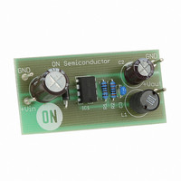
EVAL BOARD FOR LM2594APDBCKG
Manufacturer
ON Semiconductor
Specifications of LM2594APDBCKGEVB
Design Resources
LM2594APDBCKGEVB BOM LM2594APDBCKGEVB Schematic LM2594APDBCKGEVB Gerber Files
Main Purpose
DC/DC, Step Down
Outputs And Type
1, Non-Isolated
Voltage - Output
5V
Current - Output
500mA
Voltage - Input
4.5 ~ 40 V
Regulator Topology
Buck
Frequency - Switching
150kHz
Board Type
Fully Populated
Utilized Ic / Part
LM2594
Lead Free Status / RoHS Status
Lead free / RoHS Compliant
Power - Output
-
Lead Free Status / Rohs Status
Lead free / RoHS Compliant
For Use With/related Products
LM2594APDBCKG
Other names
LM2594ADPBCKGEVB
LM2594ADPBCKGEVBOS
LM2594APDBCKGEVBOS
LM2594ADPBCKGEVBOS
LM2594APDBCKGEVBOS


total package power dissipation for this switcher is quite
low, ranging from approximately 0.1 W up to 0.75 W under
varying conditions. In a carefully engineered printed circuit
board, the through−hole DIP package can easily dissipate up
to 0.75 W, even at ambient temperatures of 60°C, and still
keep the maximum junction temperature below 125°C.
Thermal Analysis and Design
the operating junction temperature. First determine:
1. P
2. T
3. T
4. R
5. R
(Refer to Maximum Ratings on page 3 of this data sheet or
R
ADDITIONAL APPLICATIONS
Inverting Regulator
LM2594−ADJ is shown in Figure 23. This circuit converts
a positive input voltage to a negative output voltage with a
common ground by bootstrapping the regulators ground to
qJC
Since the current rating of the LM2594 is only 0.5 A, the
The following procedure must be performed to determine
An
junction−ambient.
D(max)
A(max
J(max)
qJC
qJA
and R
inverting
)
qJA
maximum regulator power dissipation in the
application.
maximum ambient temperature in the
application.
maximum allowed junction temperature
(125°C for the LM2594). For a conservative
design, the maximum junction temperature
should not exceed 110°C to assure safe
operation. For every additional +10°C
temperature rise that the junction must
withstand, the estimated operating lifetime
of the component is halved.
package thermal resistance junction−case.
package thermal resistance
values).
buck−boost
Unregulated
100 mF/50 V
12 to 25 V
DC Input
C
in
regulator
Figure 23. Inverting Buck−Boost Develops −12 V
+V
in
ON/OFF
using
LM2594
http://onsemi.com
the
GND
17
Feedback
total power dissipated by the LM2594:
where d is the duty cycle and for buck converter
I
V
V
I
turn−off can be neglected if proper type catch diode is used.
following expression:
where (R
caused by the dissipated power and T
ambient temperature.
Some Aspects That can Influence Thermal Design
the junction temperature rise numbers are all approximate,
and there are many factors that will affect these numbers,
such as PC board size, shape, thickness, physical position,
location, board temperature, as well as whether the
surrounding air is moving or still.
area, copper thickness, single− or double−sided, multilayer
board, the amount of solder on the board or even color of the
traces.
board can also influence its effectiveness to dissipate the heat.
the negative output voltage. By grounding the feedback pin,
the regulator senses the inverted output voltage and
regulates it.
output. The maximum input voltage in this case cannot
exceed +28 V because the maximum voltage appearing
Q
Load
in
D1
1N5819
O
The following formula is to calculate the approximate
The dynamic switching losses during turn−on and
The junction temperature can be determined by the
It should be noted that the package thermal resistance and
Other factors are trace width, total printed circuit copper
The size, quantity and spacing of other components on the
In this example the LM2594 is used to generate a −12 V
100 mH
L1
(quiescent current) and V
LM2594 data sheet,
is minimum input voltage applied,
is the regulator output voltage,
is the load current.
qJA
C
220 mF
)(P
out
P
D
D
= (V
) represents the junction temperature rise
T
J
R3
in
d +
= (R
x I
−12 V @ 0.7 A
C
R4
Q
t on
qJA
Regulated
FF
T
) + d x I
Output
) (P
+
sat
V
V in
D
) + T
O
can be found in the
Load
,
A
x V
A
is the maximum
sat
Related parts for LM2594APDBCKGEVB
Image
Part Number
Description
Manufacturer
Datasheet
Request
R

Part Number:
Description:
ON Semiconductor [VOLTAGE REGULATOR]
Manufacturer:
ON Semiconductor
Datasheet:
Part Number:
Description:
357-036-542-201 CARDEDGE 36POS DL .156 BLK LOPRO
Manufacturer:
ON Semiconductor
Datasheet:
Part Number:
Description:
357-036-542-201 CARDEDGE 36POS DL .156 BLK LOPRO
Manufacturer:
ON Semiconductor
Datasheet:
Part Number:
Description:
357-036-542-201 CARDEDGE 36POS DL .156 BLK LOPRO
Manufacturer:
ON Semiconductor
Datasheet:
Part Number:
Description:
357-036-542-201 CARDEDGE 36POS DL .156 BLK LOPRO
Manufacturer:
ON Semiconductor
Datasheet:
Part Number:
Description:
357-036-542-201 CARDEDGE 36POS DL .156 BLK LOPRO
Manufacturer:
ON Semiconductor
Datasheet:
Part Number:
Description:
357-036-542-201 CARDEDGE 36POS DL .156 BLK LOPRO
Manufacturer:
ON Semiconductor
Datasheet:
Part Number:
Description:
357-036-542-201 CARDEDGE 36POS DL .156 BLK LOPRO
Manufacturer:
ON Semiconductor
Datasheet:
Part Number:
Description:
357-036-542-201 CARDEDGE 36POS DL .156 BLK LOPRO
Manufacturer:
ON Semiconductor
Datasheet:
Part Number:
Description:
357-036-542-201 CARDEDGE 36POS DL .156 BLK LOPRO
Manufacturer:
ON Semiconductor
Datasheet:
Part Number:
Description:
357-036-542-201 CARDEDGE 36POS DL .156 BLK LOPRO
Manufacturer:
ON Semiconductor
Datasheet:
Part Number:
Description:
Manufacturer:
ON Semiconductor
Datasheet:
Part Number:
Description:
Manufacturer:
ON Semiconductor
Datasheet:
Part Number:
Description:
Manufacturer:
ON Semiconductor
Datasheet: