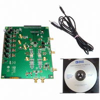
AD9117-EBZ Analog Devices Inc, AD9117-EBZ Datasheet - Page 17

AD9117-EBZ
Manufacturer Part Number
AD9117-EBZ
Description
BOARD EVALUATION FOR AD9117
Manufacturer
Analog Devices Inc
Series
TxDAC®r
Datasheet
1.AD9114BCPZ.pdf
(80 pages)
Specifications of AD9117-EBZ
Number Of Dac's
2
Number Of Bits
14
Outputs And Type
2, Differential
Sampling Rate (per Second)
125M
Data Interface
Serial
Dac Type
Current
Voltage Supply Source
Analog and Digital
Operating Temperature
-40°C ~ 85°C
Utilized Ic / Part
AD9117
Lead Free Status / RoHS Status
Lead free / RoHS Compliant
Pin No.
31
32
33
34
35
36
37
38
39
40
Mnemonic
CMLI
FSADJQ/AUXQ
FSADJI/AUXI
REFIO
RESET/PINMD
SCLK/CLKMD
SDIO/FORMAT
CS/PWRDN
DB13 (MSB)
DB12
EP (EPAD)
Description
I DAC Output Common-Mode Level. When the internal on-chip (IR
the on-chip IR
is disabled, this pin is the common-mode load for I DAC and must be connected to AVSS through a resistor,
see the Using the Internal Termination Resistors section. Recommended value for this external resistor is 0 Ω.
Full-Scale Current Output Adjust (FSADJQ). When the internal on chip (QR
scale current output adjust for Q DAC and must be connected to AVSS through a resistor, see the Theory of
Operation section. Nominal value for this external resistor is 4 kΩ for 8 mA output current.
Auxiliary Q DAC Output (AUXQ). When the internal on-chip (QR
Full-Scale Current Output Adjust (FSADJI). When the internal on-chip (IR
current output adjust for I DAC and must be connected to AVSS through a resistor, see the Theory of Operation
section. Nominal value for this external resistor is 4 kΩ for 8 mA output current.
Auxiliary I DAC Output (AUXI). When the internal on-chip (IR
Reference Input/Output. Serves as a reference input when the internal reference is disabled. Provides a 1.0 V
reference output when in internal reference mode (a 0.1 μF capacitor to AVSS is required).
This pin defines the operation mode of the part. A logic low (pull-down to DVSS) sets the part in SPI mode.
Pulse RESET high to reset the SPI registers to their default values.
A logic high (pull-up to DVDDIO) puts the device into pin mode (PINMD).
Clock Input for Serial Port (SCLK). In SPI mode, this pin is the clock input for the serial port.
Clock Mode (CLKMD). In pin mode, CLKMD determines the phase of the internal retiming clock. When
DCLKIO = CLKIN, tie it to 0. When DCLKIO ≠ CLKIN, pulse 0 to 1 to edge trigger the internal retime, see
the Retimer section.
Serial Port Input/Output (SDIO). In SPI mode, this pin is the bidirectional data line for the serial port.
Format Pin (FORMAT). In pin mode, FORMAT determines the data format of digital data. A logic low
(pull-down to DVSS) selects the binary input data format. A logic high (pull-up to DVDDIO) selects the
twos complement input data format.
Active Low Chip Select (CS). In SPI mode, this pin serves as the active low chip select.
Power-Down (PWRDN). In pin mode, a logic high (pull-up to DVDDIO) powers down the device, except for
the SPI port.
Digital Input (MSB).
Digital Input.
The exposed pad is connected to AVSS and must be soldered to the ground plane. Exposed metal at the
package corners is connected to this pad.
CML
resistor. It is recommended to leave this pin unconnected. When the internal on-chip (IR
Rev. A | Page 17 of 80
AD9114/AD9115/AD9116/AD9117
SET
SET
) is enabled, this pin is the auxiliary Q DAC output.
) is enabled, it is the auxiliary I DAC output.
CML
) is enabled, this pin is connected to
SET
SET
) is disabled, this pin is the full-scale
) is disabled, this pin is the full-
CML
)


