AD9117-EBZ Analog Devices Inc, AD9117-EBZ Datasheet - Page 31
AD9117-EBZ
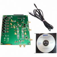
Manufacturer Part Number
AD9117-EBZ
Description
BOARD EVALUATION FOR AD9117
Manufacturer
Analog Devices Inc
Series
TxDAC®r
Datasheet
1.AD9114BCPZ.pdf
(80 pages)
Specifications of AD9117-EBZ
Number Of Dac's
2
Number Of Bits
14
Outputs And Type
2, Differential
Sampling Rate (per Second)
125M
Data Interface
Serial
Dac Type
Current
Voltage Supply Source
Analog and Digital
Operating Temperature
-40°C ~ 85°C
Utilized Ic / Part
AD9117
Lead Free Status / RoHS Status
Lead free / RoHS Compliant


TERMINOLOGY
Linearity Error or Integral Nonlinearity (INL)
Linearity error is defined as the maximum deviation of the
actual analog output from the ideal output, determined by
a straight line drawn from zero scale to full scale.
Differential Nonlinearity (DNL)
DNL is the measure of the variation in analog value, normalized
to full scale, associated with a 1 LSB change in digital input code.
Monotonicity
A DAC is monotonic if the output either increases or remains
constant as the digital input increases.
Offset Error
Offset error is the deviation of the output current from the ideal
of zero. For I
are all 0. For I
are set to 1.
Gain Error
Gain error is the difference between the actual and the ideal
output span. The actual span is determined by the difference
between the output when all inputs are set to 1 and the output
when all inputs are set to 0.
Output Compliance Range
The output compliance range is the range of allowable voltage at
the output of a current output DAC. Operation beyond the
maximum compliance limits can cause either output stage
saturation or breakdown, resulting in nonlinear performance.
Temperature Drift
Temperature drift is specified as the maximum change from
the ambient value (25°C) to the value at either T
For offset and gain drift, the drift is reported in ppm of full-
scale range per degree Celsius (ppm FSR/°C). For reference
drift, the drift is reported in parts per million per degree
Celsius (ppm/°C).
OUTP
OUTN
, the 0 mA output is expected when the inputs
, the 0 mA output is expected when all inputs
MIN
or T
MAX
.
Rev. A | Page 31 of 80
Power Supply Rejection
Power supply rejection is the maximum change in the full-scale
output as the supplies are varied from minimum to maximum
specified voltages.
Settling Time
Settling time is the time required for the output to reach and
remain within a specified error band around its final value,
measured from the start of the output transition.
Spurious Free Dynamic Range (SFDR)
SFDR is the difference, in decibels (dB), between the peak
amplitude of the output signal and the peak spurious signal
between dc and the frequency equal to half the input data rate.
Total Harmonic Distortion (THD)
THD is the ratio of the rms sum of the first six harmonic
components to the rms value of the measured fundamental.
It is expressed as a percentage (%) or in decibels (dB).
Signal-to-Noise Ratio (SNR)
SNR is the ratio of the rms value of the measured output signal
to the rms sum of all other spectral components below the Nyquist
frequency, excluding the first six harmonics and dc. The value
for SNR is expressed in decibels (dB).
Adjacent Channel Leakage Ratio (ACLR)
ACLR is the ratio in decibels relative to the carrier (dBc)
between the measured power within a channel relative to
its adjacent channel.
Complex Image Rejection
In a traditional two-part upconversion, two images are created
around the second IF frequency. These images have the effect
of wasting transmitter power and system bandwidth. By placing
the real part of a second complex modulator in series with the
first complex modulator, either the upper or lower frequency
image near the second IF can be rejected.
AD9114/AD9115/AD9116/AD9117
Related parts for AD9117-EBZ
Image
Part Number
Description
Manufacturer
Datasheet
Request
R

Part Number:
Description:
Dual 14B, Low Power D-A Converter
Manufacturer:
Analog Devices Inc
Datasheet:

Part Number:
Description:
±1.7g Dual-Axis IMEMS Accelerometer Evaluation Board
Manufacturer:
Analog Devices Inc
Datasheet:
Part Number:
Description:
Inertial Sensor Evaluation System
Manufacturer:
Analog Devices Inc
Datasheet:
Part Number:
Description:
Manufacturer:
Analog Devices Inc
Datasheet:
Part Number:
Description:
Manufacturer:
Analog Devices Inc
Datasheet:
Part Number:
Description:
Manufacturer:
Analog Devices Inc
Datasheet:
Part Number:
Description:
Manufacturer:
Analog Devices Inc
Datasheet:
Part Number:
Description:
Manufacturer:
Analog Devices Inc
Datasheet:
Part Number:
Description:
Manufacturer:
Analog Devices Inc
Datasheet:
Part Number:
Description:
Manufacturer:
Analog Devices Inc
Datasheet:
Part Number:
Description:
Manufacturer:
Analog Devices Inc
Datasheet:
Part Number:
Description:
Manufacturer:
Analog Devices Inc
Datasheet:
Part Number:
Description:
Manufacturer:
Analog Devices Inc
Datasheet: