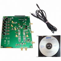
AD9117-EBZ Analog Devices Inc, AD9117-EBZ Datasheet - Page 42
AD9117-EBZ
Manufacturer Part Number
AD9117-EBZ
Description
BOARD EVALUATION FOR AD9117
Manufacturer
Analog Devices Inc
Series
TxDAC®r
Datasheet
1.AD9114BCPZ.pdf
(80 pages)
Specifications of AD9117-EBZ
Number Of Dac's
2
Number Of Bits
14
Outputs And Type
2, Differential
Sampling Rate (per Second)
125M
Data Interface
Serial
Dac Type
Current
Voltage Supply Source
Analog and Digital
Operating Temperature
-40°C ~ 85°C
Utilized Ic / Part
AD9117
Lead Free Status / RoHS Status
Lead free / RoHS Compliant


AD9114/AD9115/AD9116/AD9117
Table 15. Timer Register List
Bit Name
CLKMODEQ[1:0]
Searching
Reacquire
CLKMODEN
CLKMODEI[1:0]
Table 16. CLKMODEI/CLKMODEQ Details
CLKMODEI[1:0]/CLKMODEQ[1:0]
00
01
10
11
When RESET is pulsed high and then returns low (the part is in
SPI mode), the retimer runs and automatically selects a suitable
clock phase for the RETIMER-CLK within 128 clock cycles. The
SPI searching bit, Bit 4 of SPI Address 0x14, returns to low,
indicating that the retimer has locked and the part is ready for
use. The reacquire bit, Bit 3 of SPI Address 0x14, can be used to
reinitiate phase detection in the I and Q retimers at any time.
CLKMODEQ[1:0] and CLKMODEI[1:0] bits of SPI Address 0x14
provide readback for the values picked by the internal phase
detectors in the retimer (see Table 16).
To force the two retimers (I and Q) to pick a particular phase
for the retimer clock (they must both be forced to the same value),
CLKMODEN, Bit 2 of the SPI Address 0x14, should be set high
and the required phase value is written into CLKMODEI[1:0].
For example, if the DCLKIO and the CLKIN are in phase to first
order, the user could safely force the retimers to pick Phase 2 for
the RETIMER-CLK. This forcing function may be useful for
synchronizing multiple devices.
In pin mode, it is expected that the user tie CLKIN and DCLKIO
together. The device has a small amount of programmable func-
tionality using the now unused SPI pins (SCLK, SDIO, and CS ).
If the two chip clocks are tied together, the SCLK pin can be
tied to ground, and the chip uses a clock for the retimer that is
180° out of phase with the two input clocks (that is, Phase 2,
which is the safest and best option). The chip has an additional
option in pin mode when the redefined SCLK pin is high. Use
this mode if using pin mode, but CLKIN and DCLKIO are not
tied together (that is, not in phase). Holding SCLK high causes
the internal clock detector to use the phase detector output to
determine which clock to use in the retimer (that is, select a
suitable RETIMER-CLK phase). The action of taking SCLK
high causes the internal phase detector to reexamine the two
clocks and determine the relative phase. Whenever the user
wants to reevaluate the relative phase of the two clocks, the
SCLK pin can be taken low and then high again.
Description
Q datapath retimer clock selected output. Valid after the searching bit goes low.
High indicates that the internal datapath retimer is searching for the clock relationship (DAC is not usable until it is low again).
Changing this bit from 0 to 1 causes the datapath retimer circuit to reacquire the clock relationship.
0: Uses the CLKMODEI/CLKMODEQ values (as computed by the two internal retimers) for I and Q clocking.
1: Uses the CLKMODE value set in CLKMODEI[1:0] to override the bits for both the I and Q retimers (that is, force the retimer).
I datapath retimer clock selected output. Valid after searching goes low. If CLKMODEN = 1, a value written to this
register overrides both I and Q automatic retimer values.
DCLKIO-to-CLKIN Phase Relationship
0° to 90°
90° to 180°
180° to 270°
270° to 360°
Rev. A | Page 42 of 80
ESTIMATING THE OVERALL DAC PIPELINE DELAY
DAC pipeline latency is affected by the phase of the RETIMER-
CLK that is selected. If latency is critical to the system and must be
constant, the retimer should be forced to a particular phase and
not be allowed to automatically select a phase each time.
Consider the case in which DCLKIO = CLKIN (that is, in
phase), and the RETIMER-CLK is forced to Phase 2. Assume
that IRISING is 1 (that is, Q data is latched on the rising edge
and I data is latched on the falling edge). Then the latency to the
output for the I channel is three clock cycles (D-FF 1, D-FF 3, and
D-FF 4, but not D-FF 2, because it is latched on the half clock
cycle or 180°). The latency to the output for the Q channel from
the time the falling edge latches it at the pads in D-FF 0 is 2.5
clock cycles (½ clock cycle to D-FF 1, 1 clock cycle to D-FF 3, and
1 clock cycle to D-FF 4). This latency for the AD9114/AD9115/
AD9116/AD9117 is case specific and needs to be calculated based
on the RETIMER-CLK phase that is automatically selected or
manually forced.
RETIMER-CLK Selected
Phase 2
Phase 3
Phase 3
Phase 1
Related parts for AD9117-EBZ
Image
Part Number
Description
Manufacturer
Datasheet
Request
R

Part Number:
Description:
Dual 14B, Low Power D-A Converter
Manufacturer:
Analog Devices Inc
Datasheet:

Part Number:
Description:
±1.7g Dual-Axis IMEMS Accelerometer Evaluation Board
Manufacturer:
Analog Devices Inc
Datasheet:
Part Number:
Description:
Inertial Sensor Evaluation System
Manufacturer:
Analog Devices Inc
Datasheet:
Part Number:
Description:
Manufacturer:
Analog Devices Inc
Datasheet:
Part Number:
Description:
Manufacturer:
Analog Devices Inc
Datasheet:
Part Number:
Description:
Manufacturer:
Analog Devices Inc
Datasheet:
Part Number:
Description:
Manufacturer:
Analog Devices Inc
Datasheet:
Part Number:
Description:
Manufacturer:
Analog Devices Inc
Datasheet:
Part Number:
Description:
Manufacturer:
Analog Devices Inc
Datasheet:
Part Number:
Description:
Manufacturer:
Analog Devices Inc
Datasheet:
Part Number:
Description:
Manufacturer:
Analog Devices Inc
Datasheet:
Part Number:
Description:
Manufacturer:
Analog Devices Inc
Datasheet:
Part Number:
Description:
Manufacturer:
Analog Devices Inc
Datasheet: