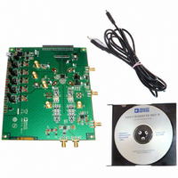
AD9117-EBZ Analog Devices Inc, AD9117-EBZ Datasheet - Page 46
AD9117-EBZ
Manufacturer Part Number
AD9117-EBZ
Description
BOARD EVALUATION FOR AD9117
Manufacturer
Analog Devices Inc
Series
TxDAC®r
Datasheet
1.AD9114BCPZ.pdf
(80 pages)
Specifications of AD9117-EBZ
Number Of Dac's
2
Number Of Bits
14
Outputs And Type
2, Differential
Sampling Rate (per Second)
125M
Data Interface
Serial
Dac Type
Current
Voltage Supply Source
Analog and Digital
Operating Temperature
-40°C ~ 85°C
Utilized Ic / Part
AD9117
Lead Free Status / RoHS Status
Lead free / RoHS Compliant


AD9114/AD9115/AD9116/AD9117
Fine Gain
Each main DAC has independent fine gain control using the
lower six bits in Register 0x03 (I DACGAIN[5:0]) and Register
0x06 (Q DACGAIN[5:0]). Unlike Coarse Gain Option 1, this
impacts only the main DAC full-scale output current. These
registers use straight binary format. One application in which
straight binary format is critical is for side-band suppression
while using a quadrature modulator. This is described in more
detail in the Applications Information section.
USING THE INTERNAL TERMINATION RESISTORS
The AD9117/AD9116/AD9115/AD9114 have four 62.5 Ω
termination internal resistors (two for each DAC output).
To use these resistors to convert the DAC output current to a
voltage, connect each DAC output pin to the adjacent load pin.
For example, on the I DAC, IOUTP must be shorted to RLIP
and IOUTN must be shorted to RLIN. In addition, the CMLI
or CMLQ pin must be connected to ground directly or through
a resistor. If the output current is at the nominal 20 mA and the
CMLI or CMLQ pin is tied directly to ground, this produces a
dc common-mode bias voltage on the DAC output equal to 0.5 V.
If the DAC dc bias must be higher than 0.5 V, an external
resistor can be connected between the CMLI or CMLQ pin and
ground. This part also has an internal common-mode resistor
that can be enabled. This is explained in the Using the Internal
Common-Mode Resistor section.
11.10
11.00
10.90
10.80
10.70
10.60
10.50
0
3.3V DAC1
3.3V DAC2
1.8V DAC1
1.8V DAC2
Figure 100. Simplified Internal Load Options
Figure 99. Typical DAC Gain Characteristics
8
Q DAC
I DAC
OR
16
xR
CM
24
GAIN DAC CODE
CML
62.5Ω
62.5Ω
32
40
RLIN
IOUTN
IOUTP
RLIP
48
56
64
Rev. A | Page 46 of 80
Using the Internal Common-Mode Resistor
These devices contain an adjustable internal common-mode
resistor that can be used to increase the dc bias of the DAC
outputs. By default, the common-mode resistor is not connected.
When enabled, it can be adjusted from ~60 Ω to ~260 Ω. Each
main DAC has an independent adjustment using the lower six bits
in Register 0x05 (IRCML[5:0]) and Register 0x08 (QRCML[5:0]).
Using the CMLx Pins for Optimal Performance
The CMLx pins also serve to change the DAC bias voltages in
the parts allowing them to run at higher dc output bias voltages.
When running the bias voltage below 0.9 V and an AVDD of
3.3 V, the parts perform optimally when the CMLx pins are tied
to ground. When the dc bias increases above 0.9 V, set the CMLx
pins at 0.5 V for optimal performance. The maximum dc bias
on the DAC output should be kept at or below 1.2 V when the
supply is 3.3 V. When the supply is 1.8 V, keep the dc bias close
to 0 V and connect the CMLx pins directly to ground.
260
240
220
200
180
160
140
120
100
80
60
Figure 101. Typical CML Resistor Value vs. Register Code
0
8
16
24
CODE
32
40
48
56
Related parts for AD9117-EBZ
Image
Part Number
Description
Manufacturer
Datasheet
Request
R

Part Number:
Description:
Dual 14B, Low Power D-A Converter
Manufacturer:
Analog Devices Inc
Datasheet:

Part Number:
Description:
±1.7g Dual-Axis IMEMS Accelerometer Evaluation Board
Manufacturer:
Analog Devices Inc
Datasheet:
Part Number:
Description:
Inertial Sensor Evaluation System
Manufacturer:
Analog Devices Inc
Datasheet:
Part Number:
Description:
Manufacturer:
Analog Devices Inc
Datasheet:
Part Number:
Description:
Manufacturer:
Analog Devices Inc
Datasheet:
Part Number:
Description:
Manufacturer:
Analog Devices Inc
Datasheet:
Part Number:
Description:
Manufacturer:
Analog Devices Inc
Datasheet:
Part Number:
Description:
Manufacturer:
Analog Devices Inc
Datasheet:
Part Number:
Description:
Manufacturer:
Analog Devices Inc
Datasheet:
Part Number:
Description:
Manufacturer:
Analog Devices Inc
Datasheet:
Part Number:
Description:
Manufacturer:
Analog Devices Inc
Datasheet:
Part Number:
Description:
Manufacturer:
Analog Devices Inc
Datasheet:
Part Number:
Description:
Manufacturer:
Analog Devices Inc
Datasheet: