AD9785-EBZ Analog Devices Inc, AD9785-EBZ Datasheet - Page 44
AD9785-EBZ
Manufacturer Part Number
AD9785-EBZ
Description
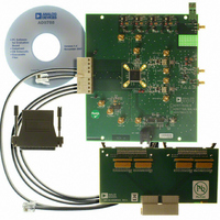
BOARD EVAL FOR AD9785
Manufacturer
Analog Devices Inc
Series
TxDAC®r
Datasheet
1.AD9785BSVZ.pdf
(64 pages)
Specifications of AD9785-EBZ
Number Of Dac's
2
Number Of Bits
12
Outputs And Type
2, Differential
Sampling Rate (per Second)
800M
Data Interface
Serial
Settling Time
22ms
Dac Type
Current
Voltage Supply Source
Analog and Digital
Operating Temperature
-40°C ~ 85°C
Utilized Ic / Part
AD9785
Silicon Manufacturer
Analog Devices
Application Sub Type
DAC
Kit Application Type
Data Converter
Silicon Core Number
AD9785
Kit Contents
Board
Lead Free Status / RoHS Status
Lead free / RoHS Compliant
Lead Free Status / RoHS Status
Lead free / RoHS Compliant, Lead free / RoHS Compliant


AD9785/AD9787/AD9788
SYNCHRONIZING DEVICES TO A SYSTEM CLOCK
The AD9785/AD9787/AD9788 offer a pulse mode synchron-
ization scheme (see Figure 61) to align the DAC outputs of
multiple devices within a system to the same DAC clock edge.
The pulse mode synchronization scheme is a two-part
operation. First, the internal clocks are synchronized by
providing either a one-time pulse or periodic signal to the
SYNC_I (SYNC_I+/SYNC_I−) inputs. The SYNC_I signal is
sampled by the internal DACCLK sample rate clock.
The SYNC_I input frequency has the following two constraints:
where N is an integer.
When the internal clocks are synchronized, the data sampling
clocks between all devices are phase aligned. The next step
requires a simultaneous strobe signal to the TXENABLE pin of
all devices that is synchronous to the DATACLK signal. This
resets the phase accumulator of the NCOs across all devices,
effectively synchronizing the NCOs. The strobe signal is
sampled by f
times as the input data. Because the TXENABLE pin is an active
f
f
SYNC
SYNC
_
_
IN
IN
DATACLK
16
f
DATACLK
f
DAC
and must meet the same setup and hold
N
TXENABLE
DATACLK
REFCLK
DACCLK
REFCLK
SYNC_I
Figure 63. Timing Diagram of TXENABLE vs. DATACLK and REFCLK
Figure 62. Timing Diagram of SYNC_I with Respect to REFCLK
t
t
SDATACLK
SREFCLK
Rev. A | Page 44 of 64
t
S_SYNC
high logic level pin, the strobe signal should be a low logic level
pulse unless the TXENABLE invert bit is set in the SPI.
For this synchronization scheme, all devices are slave devices,
while the system clock generation/distribution chip serves as
the master. The external LVDS signal should be connected to the
SYNC_I inputs of all the slave devices following the constraints.
The DAC clock inputs and the SYNC_I inputs must be matched
in length across all devices.
It is vital that the SYNC_I signal be distributed between the
DACs with low skew. Likewise, the REFCLK signals must be
distributed with low skew. Any skew on these signals between
the DACs must be accounted for in the timing budget. The
SYNC_I signal is sampled at the DACCLK rate, thus the data
valid window of the SYNC_I pulse must be presented to all the
DACs within the same DACCLK period.
Figure 62 shows the timing of the SYNC_I input with respect to
the REFCLK input. Note that although the timing is relative to
the REFCLK signal, SYNC_I is sampled at the DACCLK rate.
This means that the rising edge of the SYNC_I signal must
occur after the hold time of the preceding DACCLK rising edge
and not the preceding REFCLK rising edge. Figure 63 shows a
timing diagram of the TXENABLE input.
t
H_SYNC
t
t
HDATACLK
HREFCLK
Related parts for AD9785-EBZ
Image
Part Number
Description
Manufacturer
Datasheet
Request
R

Part Number:
Description:
Dual 16B, 1.0 GSPS TxDAC
Manufacturer:
Analog Devices Inc
Datasheet:

Part Number:
Description:
±1.7g Dual-Axis IMEMS Accelerometer Evaluation Board
Manufacturer:
Analog Devices Inc
Datasheet:
Part Number:
Description:
Inertial Sensor Evaluation System
Manufacturer:
Analog Devices Inc
Datasheet:
Part Number:
Description:
Manufacturer:
Analog Devices Inc
Datasheet:
Part Number:
Description:
Manufacturer:
Analog Devices Inc
Datasheet:
Part Number:
Description:
Manufacturer:
Analog Devices Inc
Datasheet:
Part Number:
Description:
Manufacturer:
Analog Devices Inc
Datasheet:
Part Number:
Description:
Manufacturer:
Analog Devices Inc
Datasheet:
Part Number:
Description:
Manufacturer:
Analog Devices Inc
Datasheet:
Part Number:
Description:
Manufacturer:
Analog Devices Inc
Datasheet:
Part Number:
Description:
Manufacturer:
Analog Devices Inc
Datasheet:
Part Number:
Description:
Manufacturer:
Analog Devices Inc
Datasheet:
Part Number:
Description:
Manufacturer:
Analog Devices Inc
Datasheet: