AD9785-EBZ Analog Devices Inc, AD9785-EBZ Datasheet - Page 47
AD9785-EBZ
Manufacturer Part Number
AD9785-EBZ
Description
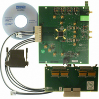
BOARD EVAL FOR AD9785
Manufacturer
Analog Devices Inc
Series
TxDAC®r
Datasheet
1.AD9785BSVZ.pdf
(64 pages)
Specifications of AD9785-EBZ
Number Of Dac's
2
Number Of Bits
12
Outputs And Type
2, Differential
Sampling Rate (per Second)
800M
Data Interface
Serial
Settling Time
22ms
Dac Type
Current
Voltage Supply Source
Analog and Digital
Operating Temperature
-40°C ~ 85°C
Utilized Ic / Part
AD9785
Silicon Manufacturer
Analog Devices
Application Sub Type
DAC
Kit Application Type
Data Converter
Silicon Core Number
AD9785
Kit Contents
Board
Lead Free Status / RoHS Status
Lead free / RoHS Compliant
Lead Free Status / RoHS Status
Lead free / RoHS Compliant, Lead free / RoHS Compliant


DRIVING THE REFCLK INPUT
The REFCLK input requires a low jitter differential drive signal.
REFCLK is a PMOS input differential pair powered from the 1.8 V
supply; therefore, it is important to maintain the specified 400 mV
input common-mode voltage. Each input pin can safely swing
from 200 mV p-p to 1 V p-p about the 400 mV common-mode
voltage. Although these input levels are not directly LVDS-
compatible, REFCLK can be driven by an offset ac-coupled
LVDS signal, as shown in Figure 65.
If a clean sine clock is available, it can be transformer-coupled
to REFCLK, as shown in Figure 66. Use of a CMOS or TTL
clock is also acceptable for lower sample rates. It can be routed
through a CMOS-to-LVDS translator, then ac-coupled.
A simple bias network for generating V
It is important to use CVDD18 and CGND for the clock bias
circuit. Any noise or other signal that is coupled onto the clock
is multiplied by the DAC digital input signal and can degrade
DAC performance.
DAC REFCLK CONFIGURATION
The AD9785/AD9787/AD9788 offer two modes of sourcing
the DAC sample clock (DACCLK). The first mode employs an
on-chip clock multiplier that accepts a reference clock operating
at the lower input frequency, most commonly the data input
frequency. The on-chip phase-locked loop (PLL) then multiplies
the reference clock up to a higher frequency, which can then be
used to generate all the internal clocks required by the DAC.
The clock multiplier provides a high quality clock that meets
the performance requirements of most applications. Using the
TTL OR CMOS
CLK INPUT
LVDS_N_IN
287
LVDS_P_IN
1k
Ω
Ω
Figure 66. TTL or CMOS REFCLK Drive Circuit
Figure 67. REFCLK V
Figure 65. LVDS REFCLK Drive Circuit
0.1µF
0.1
0.1µF
0.1µF
µ
F
1nF
50Ω
50Ω
CM
Generator Circuit
V
V
CM
50Ω
50Ω
CM
CM
1nF
= 400mV
= 400mV
BAV99ZXCT
HIGH SPEED
DUAL DIODE
V
is shown in Figure 67.
CM
REFCLK+
REFCLK–
= 400mV
CVDD18
CGND
REFCLK+
REFCLK–
Rev. A | Page 47 of 64
on-chip clock multiplier removes the burden of generating and
distributing the high speed DACCLK.
The second mode bypasses the clock multiplier circuitry and
allows DACCLK to be directly sourced through the REFCLK
pins. This mode enables the user to source a very high quality
clock directly to the DAC core. Sourcing the DACCLK directly
through the REFCLK pins may be necessary in demanding
applications that require the lowest possible DAC output noise
at higher output frequencies.
In either case, using the on-chip clock multiplier or sourcing
the DACCLK directly through the REFCLK pins, it is necessary
that the REFCLK signal have low jitter to maximize the DAC
noise performance.
Direct Clocking
When the PLL is disabled (Register 0x04, Bit 15 = 0), the
REFCLK input is used directly as the DAC sample clock
(DACCLK). The output frequency of the DATACLK output
pin is
where IF is the interpolation factor, set in Register 0x01, Bits [7:6],
and P = 0.5 if in single-port mode.
Clock Multiplication
When the PLL is enabled (Register 0x04, Bit 15 = 1), the clock
multiplication circuit generates the DAC sample clock from the
lower rate REFCLK input. The functional diagram of the clock
multiplier is shown in Figure 68.
The clock multiplication circuit operates such that the VCO
outputs a frequency, f
frequency multiplied by N1 × N2.
The DAC sample clock frequency, f
The values of N1 and N2 must be chosen to keep f
optimal operating range of 1.0 GHz to 2.0 GHz. When the VCO
output frequency is known, the correct PLL band select value
(Register 0x04, Bits [7:2]) can be chosen.
PLL Bias Settings
There are three bias settings for the PLL circuitry that should be
programmed to their nominal values. The PLL values shown in
Table 34 are the recommended settings for these parameters.
Table 34. PLL Settings
PLL SPI Control
PLL Loop Bandwidth
PLL VCO Drive
PLL Bias
f
f
f
DATACLK
VCO
DACCLK
= f
= f
REFCLK
= f
REFCLK
DACCLK
× (N1 × N2)
× N2
/(IF × P)
VCO
, equal to the REFCLK input signal
AD9785/AD9787/AD9788
Register
0x04
0x04
0x04
Address
DACCLK
, is equal to
Bit
[20:16]
[1:0]
[10:8]
VCO
in the
Optimal
Setting
01111
11
011
Related parts for AD9785-EBZ
Image
Part Number
Description
Manufacturer
Datasheet
Request
R

Part Number:
Description:
Dual 16B, 1.0 GSPS TxDAC
Manufacturer:
Analog Devices Inc
Datasheet:

Part Number:
Description:
±1.7g Dual-Axis IMEMS Accelerometer Evaluation Board
Manufacturer:
Analog Devices Inc
Datasheet:
Part Number:
Description:
Inertial Sensor Evaluation System
Manufacturer:
Analog Devices Inc
Datasheet:
Part Number:
Description:
Manufacturer:
Analog Devices Inc
Datasheet:
Part Number:
Description:
Manufacturer:
Analog Devices Inc
Datasheet:
Part Number:
Description:
Manufacturer:
Analog Devices Inc
Datasheet:
Part Number:
Description:
Manufacturer:
Analog Devices Inc
Datasheet:
Part Number:
Description:
Manufacturer:
Analog Devices Inc
Datasheet:
Part Number:
Description:
Manufacturer:
Analog Devices Inc
Datasheet:
Part Number:
Description:
Manufacturer:
Analog Devices Inc
Datasheet:
Part Number:
Description:
Manufacturer:
Analog Devices Inc
Datasheet:
Part Number:
Description:
Manufacturer:
Analog Devices Inc
Datasheet:
Part Number:
Description:
Manufacturer:
Analog Devices Inc
Datasheet: