CDB4398 Cirrus Logic Inc, CDB4398 Datasheet - Page 37
CDB4398
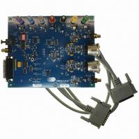
Manufacturer Part Number
CDB4398
Description
BOARD EVAL FOR CS4398 DAC
Manufacturer
Cirrus Logic Inc
Specifications of CDB4398
Number Of Dac's
2
Number Of Bits
24
Outputs And Type
2, Differential
Sampling Rate (per Second)
192k
Data Interface
I²C, SPI™
Dac Type
Voltage
Voltage Supply Source
Analog and Digital
Operating Temperature
-10°C ~ 70°C
Utilized Ic / Part
CS4398
Description/function
Audio D/A
Operating Supply Voltage
5 V
Product
Audio Modules
For Use With/related Products
CS4398
Lead Free Status / RoHS Status
Contains lead / RoHS non-compliant
Lead Free Status / RoHS Status
Lead free / RoHS Compliant, Contains lead / RoHS non-compliant
Other names
598-1155


DS568F1
7.8
7.8.1
7.8.2
7.8.3
7.8.4
7.8.5
PDN
1
7
Misc. Control - Register 08h
Power Down (PDN) Bit 7
Function:
When set to 1 (default), the entire device enters a low-power state, and the contents of the control regis-
ters is retained. The power-down bit defaults to ‘1’ on power-up and must be disabled before normal op-
eration in Control Port mode can occur. This bit is ignored if CPEN is not set.
Control Port Enable (CPEN) Bit 6
Function:
This bit is set to 0 by default, allowing the device to power-up in Stand-Alone Mode. Control Port Mode
can be accessed by setting this bit to 1. This allows operation of the device to be controlled by the regis-
ters, and the pin definitions will conform to Control Port Mode.
Freeze Controls (Freeze) Bit 5
Function:
When set to 1, this function allows modifications to be made to the registers without the changes taking
effect until FREEZE is set back to 0. To make multiple changes in the Control Port registers take effect
simultaneously, enable the FREEZE bit, make all register changes, then disable the FREEZE bit.
When set to 0 (default), register changes take effect immediately.
Master Clock Divide-by-2 ENABLE (MCLKDIV2) Bit 4
Function:
When set to 1, the MCLKDIV bit enables a circuit which divides the externally applied MCLK signal by 2
prior to all other internal circuitry.
When set to 0 (default), MCLK is unchanged.
Master Clock Divide-by-3 ENABLE (MCLKDIV3) Bit 3
Function:
When set to 1, the MCLKDIV bit enables a circuit that divides the externally applied MCLK signal by 3
prior to all other internal circuitry.
When set to 0 (default), MCLK is unchanged.
CPEN
6
0
FREEZE
5
0
MCLKDIV2
0
4
MCLKDIV3
3
0
Reserved
2
0
Reserved
0
1
Reserved
CS4398
0
0
37
Related parts for CDB4398
Image
Part Number
Description
Manufacturer
Datasheet
Request
R

Part Number:
Description:
Development Kit
Manufacturer:
Cirrus Logic Inc
Datasheet:
Part Number:
Description:
Development Kit
Manufacturer:
Cirrus Logic Inc
Datasheet:


Part Number:
Description:
High-efficiency PFC + Fluorescent Lamp Driver Reference Design
Manufacturer:
Cirrus Logic Inc
Datasheet:
Part Number:
Description:
Development Kit
Manufacturer:
Cirrus Logic Inc
Datasheet:
Part Number:
Description:
Development Kit
Manufacturer:
Cirrus Logic Inc
Datasheet:

Part Number:
Description:
Development Kit
Manufacturer:
Cirrus Logic Inc
Datasheet:
Part Number:
Description:
Development Kit
Manufacturer:
Cirrus Logic Inc
Datasheet:
Part Number:
Description:
Development Kit
Manufacturer:
Cirrus Logic Inc
Datasheet:
Part Number:
Description:
Development Kit
Manufacturer:
Cirrus Logic Inc
Datasheet:

Part Number:
Description:
EVALUATION BOARD FOR CS8427
Manufacturer:
Cirrus Logic Inc
Datasheet:

Part Number:
Description:
BOARD EVAL FOR CS8416 RCVR
Manufacturer:
Cirrus Logic Inc
Datasheet:

Part Number:
Description:
EVALUATION BOARD FOR CS8420
Manufacturer:
Cirrus Logic Inc
Datasheet:

Part Number:
Description:
KIT DEVELOPMENT EP9315 ARM9
Manufacturer:
Cirrus Logic Inc
Datasheet:

Part Number:
Description:
KIT DEVELOPMENT EP9302 ARM9
Manufacturer:
Cirrus Logic Inc
Datasheet: