DK86060-3 Fujitsu Semiconductor America Inc, DK86060-3 Datasheet - Page 5
DK86060-3
Manufacturer Part Number
DK86060-3
Description
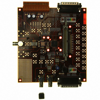
KIT DEV 16BIT DAC FOR MB86060
Manufacturer
Fujitsu Semiconductor America Inc
Specifications of DK86060-3
Number Of Dac's
1
Number Of Bits
16
Outputs And Type
1, Differential
Sampling Rate (per Second)
400M
Data Interface
Parallel
Dac Type
Current
Voltage Supply Source
Single
Operating Temperature
-40°C ~ 85°C
Utilized Ic / Part
MB86060
Lead Free Status / RoHS Status
Lead free / RoHS Compliant
Other names
865-1009


February 2009 Version 2.0
FME/MS/SFDAC1/DS/4250
MB86060 16-bit Interpolating Digital to Analog Converter
1.2
The MB86060 incorporates a clock multiplier. This may be used to generate the internal x1, x2 and
x4 clock signals required to clock the DAC core when the interpolation filters are enabled, or as a
general purpose clock multiplier to allow lower frequency clock sources to be used.
The clock multiplier is based on a delay-lock-loop whose delay is adjusted by a charge pump
controlled by a phase detector. A ‘Lock’ indicator pin is provided so that the system can monitor the
multiplier’s condition.
For systems where a high frequency clock is available, or the lowest possible jitter is required, the
clock multiplier should be disabled and an external clock applied directly as the clock multipliers
systematic jitter will cause jitter spurs to appear in the analog output
1.2.1
The input clock is selectable between either a differential system clock, typically a sine wave source
of amplitude 0dBm, or an external crystal using the internal oscillator circuit. A CMOS single ended
clock can also be connected to XIN. See Table 1 for details of these configurations.
The differential input clock pins CLK and CLKB are internally biased to have a common mode level
equivalent to the voltage applied to pin VREF. When using either the internal oscillator or an external
single ended clock connected to XIN, pins CLK and CLKB should be linked to CVSS.
If minimum jitter is required, then the differential clock should be used, with an amplitude sufficient to
ensure that the specification for minimum slew rate is met. For a 250MHz clock this represents 0dBm,
with higher amplitudes required for lower clock rates. A sine signal is recommended over a square
wave to avoid unwanted harmonics.
Copyright © 2003-2009 Fujitsu Microelectronics Europe GmbH
Disclaimer: The contents of this document are subject to change without notice. Customers are advised to consult with FUJITSU sales representatives before
CLKSEL
0
1
Clock
ordering.The information and circuit diagrams in this document are presented “as is”, no license is granted by implication or otherwise.
When using the internal oscillator with an external crystal, or connecting a single-ended
CMOS clock to XIN, the clock multiplier must be set to multiply modes x2 to x8 so that XIN
is enabled. The operating speed of the internal crystal oscillator circuit is limited. See
section 5.5.
Input Clock
Clock multiplier
x1 (either filter)
or x2 to x8
mode
Any
Table 1: Input Clock Source Selection
Differential
oscillator
source
Crystal
Clock
clock
Connect differential clock source to CLK and
Connect crystal between XIN and XOUT, or
connect CMOS clock to XIN
Production
Function
CLKB
Page 5 of 44
Related parts for DK86060-3
Image
Part Number
Description
Manufacturer
Datasheet
Request
R

Part Number:
Description:
IC POWER SUPPLY MONITOR 8SOP
Manufacturer:
Fujitsu Semiconductor America Inc
Datasheet:
Part Number:
Description:
IC POWER SUPPLY MONITOR 8SOP
Manufacturer:
Fujitsu Semiconductor America Inc
Datasheet:

Part Number:
Description:
IC MCU 60K FLASH 2KB RAM 52LQFP
Manufacturer:
Fujitsu Semiconductor America Inc
Datasheet:

Part Number:
Description:
IC MCU 32BIT 256KB FLASH 120LQFP
Manufacturer:
Fujitsu Semiconductor America Inc
Datasheet:
Part Number:
Description:
IC CTLR TOUCH SENSOR 12CH 30SSOP
Manufacturer:
Fujitsu Semiconductor America Inc
Datasheet:

Part Number:
Description:
IC CTLR TOUCH SENSOR 12CH 40QFN
Manufacturer:
Fujitsu Semiconductor America Inc
Datasheet:
Part Number:
Description:
SYNTHESIZER PLL DUAL INP 20SSOP
Manufacturer:
Fujitsu Semiconductor America Inc
Datasheet:

Part Number:
Description:
SYNTHESZR PLL 1.1GHZ DUAL 16SSOP
Manufacturer:
Fujitsu Semiconductor America Inc
Datasheet:

Part Number:
Description:
IC SSCG EMI RED 8-SOIC
Manufacturer:
Fujitsu Semiconductor America Inc
Datasheet:

Part Number:
Description:
IC SSCG EMI RED 8-TSSOP
Manufacturer:
Fujitsu Semiconductor America Inc
Datasheet:

Part Number:
Description:
IC SSCG EMI RED 8-SOP
Manufacturer:
Fujitsu Semiconductor America Inc
Datasheet:

Part Number:
Description:
SYNTHESIZER PLL 2.5GHZ 16SSOP
Manufacturer:
Fujitsu Semiconductor America Inc
Datasheet:
Part Number:
Description:
SYNTHESIZER PLL 1.2GHZ 16SSOP
Manufacturer:
Fujitsu Semiconductor America Inc
Datasheet:

Part Number:
Description:
SYNTHESIZER PLL 2.5GHZ 16BCC
Manufacturer:
Fujitsu Semiconductor America Inc
Datasheet:

Part Number:
Description:
IC SSCG EMI RED 8-SOP
Manufacturer:
Fujitsu Semiconductor America Inc
Datasheet: