DC1319B-A Linear Technology, DC1319B-A Datasheet - Page 10
DC1319B-A
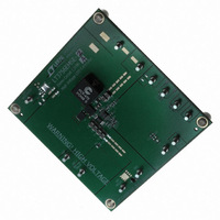
Manufacturer Part Number
DC1319B-A
Description
BOARD EVAL LED DRIVER LT3756
Manufacturer
Linear Technology
Specifications of DC1319B-A
Current - Output / Channel
500mA
Outputs And Type
1, Non-Isolated
Voltage - Output
100V
Features
Dimmable
Voltage - Input
8 ~ 80V
Utilized Ic / Part
LT3756
Lead Free Status / RoHS Status
Lead free / RoHS Compliant
Other names
DC1319A-A
DC1319A-A
DC1319A-A


operaTion
LT3756/LT3756-1/LT3756-2
The LT3756 is a constant-frequency, current mode control-
ler with a low side NMOS gate driver. The GATE pin and
PWMOUT pin drivers, and other chip loads, are powered
from INTV
the discussion that follows, it will be helpful to refer to
the Block Diagram of the IC. In normal operation, with the
PWM pin low, the GATE and PWMOUT pins are driven to
GND, the VC pin is high impedance to store the previous
switching state on the external compensation capacitor,
and the ISP and ISN pin bias currents are reduced to
leakage levels. When the PWM pin transitions high, the
PWMOUT pin transitions high after a short delay. At the
same time, the internal oscillator wakes up and gener-
ates a pulse to set the PWM latch, turning on the external
power MOSFET switch (GATE goes high). A voltage input
proportional to the switch current, sensed by an external
current sense resistor between the SENSE and GND input
pins, is added to a stabilizing slope compensation ramp
and the resulting “switch current sense” signal is fed into
the positive terminal of the PWM comparator. The current
in the external inductor increases steadily during the time
the switch is on. When the switch current sense voltage
exceeds the output of the error amplifier, labeled “VC”,
the latch is reset and the switch is turned off. During the
switch off phase, the inductor current decreases. At the
completion of each oscillator cycle, internal signals such
as slope compensation return to their starting points and a
new cycle begins with the set pulse from the oscillator.
Through this repetitive action, the PWM control algorithm
establishes a switch duty cycle to regulate a current or
voltage in the load. The VC signal is integrated over many
switching cycles and is an amplified version of the differ-
ence between the LED current sense voltage, measured
between ISP and ISN, and the target difference voltage
set by the CTRL pin. In this manner, the error amplifier
sets the correct peak switch current level to keep the
LED current in regulation. If the error amplifier output
increases, more current is demanded in the switch; if it
decreases, less current is demanded. The switch current
is monitored during the on-phase and the voltage across
the SENSE pin is not allowed to exceed the current limit
threshold of 108mV (typical). If the SENSE pin exceeds
the current limit threshold, the SR latch is reset regard-
less of the output state of the PWM comparator. Likewise,
at an ISP/ISN common mode voltage less than 3V, the
0
CC
, which is an internally regulated supply. In
difference between ISP and ISN is monitored to determine
if the output is in a short-circuit condition. If the difference
between ISP and ISN is greater than 150mV (typical), the
SR latch will be reset regardless of the PWM comparator.
These functions are intended to protect the power switch,
as well as various external components in the power path
of the DC/DC converter.
In voltage feedback mode, the operation is similar to that
described above, except the voltage at the VC pin is set
by the amplified difference of the internal reference of
1.25V (nominal) and the FB pin. If FB is lower than the
reference voltage, the switch current will increase; if FB
is higher than the reference voltage, the switch demand
current will decrease. The LED current sense feedback
interacts with the FB voltage feedback so that FB will not
exceed the internal reference and the voltage between ISP
and ISN will not exceed the threshold set by the CTRL pin.
For accurate current or voltage regulation, it is necessary
to be sure that under normal operating conditions, the
appropriate loop is dominant. To deactivate the voltage
loop entirely, FB can be connected to GND. To deactivate
the LED current loop entirely, the ISP and ISN should be
tied together and the CTRL input tied to V
Two LED specific functions featured on the LT3756 are
controlled by the voltage feedback pin. First, when the
FB pin exceeds a voltage 50mV lower (–4%) than the FB
regulation voltage, the pull-down driver on the OPENLED
pin is activated (LT3756 and LT3756-2 only). This function
provides a status indicator that the load may be discon-
nected and the constant-voltage feedback loop is taking
control of the switching regulator. When the FB pin exceeds
the FB regulation voltage by 60mV (5% typical), the PWM-
OUT pin is driven low, ignoring the state of the PWM input.
In the case where the PWMOUT pin drives a disconnect
NFET, this action isolates the LED load from GND, prevent-
ing excessive current from damaging the LEDs. If the FB
input exceeds both the open LED and the overvoltage
thresholds, then an externally driven overvoltage event
has caused the FB pin to be too high and the OPENLED
pull-down will be de-asserted. The LT3756-2 will re-assert
the OPENLED signal when FB falls below the overvoltage
threshold and remains above the open LED threshold. The
LT3756 is prevented from re-asserting OPENLED until FB
drops below both thresholds.
REF
.
375612fb
Related parts for DC1319B-A
Image
Part Number
Description
Manufacturer
Datasheet
Request
R

Part Number:
Description:
CD ROM LINEARVIEW DATASHEETS
Manufacturer:
Linear Technology

Part Number:
Description:
Standalone Linear Li-Ion Battery Charger with Thermal Regulation in ThinSOT
Manufacturer:
Linear Technology Corporation
Datasheet:
Part Number:
Description:
Low noise, high frequency, 8th order linear phase lowpass filter
Manufacturer:
Linear Technology Corporation
Datasheet:
Part Number:
Description:
Manufacturer:
Linear Technology Corporation
Datasheet:
Part Number:
Description:
Manufacturer:
Linear Technology Corporation
Datasheet:
Part Number:
Description:
Manufacturer:
Linear Technology Corporation
Datasheet:
Part Number:
Description:
Manufacturer:
Linear Technology Corporation
Datasheet:
Part Number:
Description:
Manufacturer:
Linear Technology Corporation
Datasheet:
Part Number:
Description:
Manufacturer:
Linear Technology Corporation
Datasheet:
Part Number:
Description:
Manufacturer:
Linear Technology Corporation
Datasheet:
Part Number:
Description:
Dual and Quad, JFET Input Precision High Speed Op Amps
Manufacturer:
Linear Technology Corporation
Datasheet:
Part Number:
Description:
Manufacturer:
Linear Technology Corporation
Datasheet:
Part Number:
Description:
1, 2, 6 and 8 Channel, 10-Bit Serial I/O Data Acquisition Systems
Manufacturer:
Linear Technology Corporation
Datasheet:
Part Number:
Description:
Manufacturer:
Linear Technology Corporation
Datasheet:
Part Number:
Description:
Universal dual filter building block
Manufacturer:
Linear Technology Corporation
Datasheet: