SSL2102T/DB/FLYB120V,598 NXP Semiconductors, SSL2102T/DB/FLYB120V,598 Datasheet - Page 12
SSL2102T/DB/FLYB120V,598
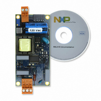
Manufacturer Part Number
SSL2102T/DB/FLYB120V,598
Description
KIT SSL2102 DESIGNER 120V
Manufacturer
NXP Semiconductors
Specifications of SSL2102T/DB/FLYB120V,598
Current - Output / Channel
400mA ~ 1.05A
Outputs And Type
1, Isolated
Voltage - Output
9 ~ 23 V
Features
Dimmable
Voltage - Input
85 ~ 276VAC
Utilized Ic / Part
SSL2102
Duty Cycle (max)
75 %
Mounting Style
SMD/SMT
Switching Frequency
100 KHz
Operating Supply Voltage
8.5 V to 40 V
Supply Current
1.7 A
Maximum Operating Temperature
+ 100 C
Minimum Operating Temperature
- 40 C
Output Power
1.6 W
Package / Case
SOIC-20
Lead Free Status / RoHS Status
Lead free / RoHS Compliant
Lead Free Status / RoHS Status
Lead free / RoHS Compliant, Lead free / RoHS Compliant
Other names
568-4931


NXP Semiconductors
UM10386
User manual
8.4 Changing the load curve
8.5 Multiple driver support
The value of the demo board weak bleeder (R6 and R7) is chosen to minimize losses
(approximately 2 W to 3 W). The weak bleeder normally only switches on during dimmed
operation. The voltage drop with some transistor dimmers is, however, not sufficient to
cause full dimming range control (minimum 10 % instead of <1 %), because the average
rectified voltage is used to determine the dimming position. To compensate for the
reduced voltage difference, voltage detection can be made more sensitive by replacing
R4 with a zener diode, such as the BZV85-C200 for 230 V (AC), or the BZV85-C68 for
120 V (AC) applications. Because of increased sensitivity, the dimming curve will also be
steeper when using triac dimmers.
The load curve can be divided into two regions: one where the control loop limits the duty
cycle of the converter, and where the output current is regulated, and another where the
duty factor feedback is no longer dominant. This last part occurs at output voltages below
13 V. In this area, constant output power becomes the dominant control mechanism.
Changing the turns ratio of the transformer to match the output load will also change the
load curve.
It is possible to attach multiple converters to a single dimmer. When using triac dimmers
the inrush current will rise, although not in proportion to the number of converters used.
Transistor dimmers are more suitable for use with multiple converters because the
dimming range will increase due to the added bleeder action, and there is no inrush
current.
Transistor dimmers contain active circuitry that require a load charge during the time
that the dimmer is open. The dimensioning of the circuit generating the internal supply
voltage inside the dimmer is made critical in order to avoid excessive internal dimmer
losses. This means that the remaining voltage drop over the lamp must be low
enough to reach this charge. For dimmers such as the Busch-Jaeger 6519U, the
minimum lamp load is specified at 40 W which is equivalent to a 1.3 kΩ resistor load
at 230 V(AC). Such a load would result in highly inefficient operation at low output
power levels, since most energy is wasted in order to drive the dimmer, and not to
produce light.
All information provided in this document is subject to legal disclaimers.
Rev. 1 — 1 February 2011
SSL2102 19 W to 22 W mains dimmable LED driver
UM10386
© NXP B.V. 2011. All rights reserved.
12 of 24
Related parts for SSL2102T/DB/FLYB120V,598
Image
Part Number
Description
Manufacturer
Datasheet
Request
R

Part Number:
Description:
KIT SSL2102 DESIGNER 230V
Manufacturer:
NXP Semiconductors
Datasheet:

Part Number:
Description:
NXP Semiconductors designed the LPC2420/2460 microcontroller around a 16-bit/32-bitARM7TDMI-S CPU core with real-time debug interfaces that include both JTAG andembedded trace
Manufacturer:
NXP Semiconductors
Datasheet:

Part Number:
Description:
NXP Semiconductors designed the LPC2458 microcontroller around a 16-bit/32-bitARM7TDMI-S CPU core with real-time debug interfaces that include both JTAG andembedded trace
Manufacturer:
NXP Semiconductors
Datasheet:
Part Number:
Description:
NXP Semiconductors designed the LPC2468 microcontroller around a 16-bit/32-bitARM7TDMI-S CPU core with real-time debug interfaces that include both JTAG andembedded trace
Manufacturer:
NXP Semiconductors
Datasheet:
Part Number:
Description:
NXP Semiconductors designed the LPC2470 microcontroller, powered by theARM7TDMI-S core, to be a highly integrated microcontroller for a wide range ofapplications that require advanced communications and high quality graphic displays
Manufacturer:
NXP Semiconductors
Datasheet:
Part Number:
Description:
NXP Semiconductors designed the LPC2478 microcontroller, powered by theARM7TDMI-S core, to be a highly integrated microcontroller for a wide range ofapplications that require advanced communications and high quality graphic displays
Manufacturer:
NXP Semiconductors
Datasheet:
Part Number:
Description:
The Philips Semiconductors XA (eXtended Architecture) family of 16-bit single-chip microcontrollers is powerful enough to easily handle the requirements of high performance embedded applications, yet inexpensive enough to compete in the market for hi
Manufacturer:
NXP Semiconductors
Datasheet:
Part Number:
Description:
The XA-S3 device is a member of Philips Semiconductors? XA(eXtended Architecture) family of high performance 16-bitsingle-chip microcontrollers
Manufacturer:
NXP Semiconductors
Datasheet:

Part Number:
Description:
The NXP BlueStreak LH75401/LH75411 family consists of two low-cost 16/32-bit System-on-Chip (SoC) devices
Manufacturer:
NXP Semiconductors
Datasheet:
Part Number:
Description:
The NXP LPC3130/3131 combine an 180 MHz ARM926EJ-S CPU core, high-speed USB2
Manufacturer:
NXP Semiconductors
Datasheet:
Part Number:
Description:
The NXP LPC3141 combine a 270 MHz ARM926EJ-S CPU core, High-speed USB 2
Manufacturer:
NXP Semiconductors
Part Number:
Description:
The NXP LPC3143 combine a 270 MHz ARM926EJ-S CPU core, High-speed USB 2
Manufacturer:
NXP Semiconductors

Part Number:
Description:
The NXP LPC3152 combines an 180 MHz ARM926EJ-S CPU core, High-speed USB 2
Manufacturer:
NXP Semiconductors
Part Number:
Description:
The NXP LPC3154 combines an 180 MHz ARM926EJ-S CPU core, High-speed USB 2
Manufacturer:
NXP Semiconductors